


APPENDIX 3 FIRMWARE SWITCHS (WSW)
A-28
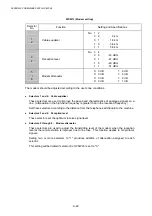
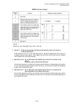
WSW21 (TAD setting 1)
Selector
No.
Function
Setting and Specifications
1
|
7
Not used.
8
Erasure of message stored in the
memory after the message
transfer
0:
Yes 1:
No
l
Selector 8: Erasure of message
Setting this selector to "0" will erase the message recorded in the memory after the document
retrieval feature transfers the message.
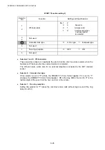
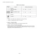
WSW22 (ECM setting)
Selector
No.
Function
Setting and Specifications
1
ECM* in sending
0: ON
1: OFF
2
ECM* in receiving
0: ON
1: OFF
3
Call Waiting Caller ID
0: ON
1: OFF
4 Not
used.
5
|
8
Not used.
* ECM: Error correction mode
NOTE:
•
Selector 3 is applicable to the American version only, but not applicable to those models
equipped with high-speed modem.
•
Selectors 5 through 8 are applicable to the Asian version only.
l
Selector 3: Call Waiting Caller ID
Setting this selector to "0" allows the user to decide whether or not to interrupt the current call
when a new call comes in. If Call Waiting Caller ID service is available in the area and the
user subscribes to it, he/she can see information about his/her incoming call.
Содержание DCP-8040
Страница 146: ...CHAPTER 4 DISASSEMBLY AND RE ASSEMBLY 4 64 5 Remove the shutter arm C Fig 4 115 Shutter arm C Frame L ...
Страница 276: ...CHAPTER 7 MAINTENANCE MODE 7 6 Fig 7 3 l m a b c d e f g h i j k ...
Страница 347: ...APPENDIX 4 CIRCUIT DIAGRAMS A 50 Appendix 4 1 Main PCB Circuit Diagram 1 7 ...
Страница 348: ...MFC 8440 8840D 8840DN DCP 8040 8045D 8045DN SERVICE MANUAL A 51 Appendix 4 2 Main PCB Circuit Diagram 2 7 ...
Страница 349: ...APPENDIX 4 CIRCUIT DIAGRAMS A 52 Appendix 4 3 Main PCB Circuit Diagram 3 7 ...
Страница 350: ...MFC 8440 8840D 8840DN DCP 8040 8045D 8045DN SERVICE MANUAL A 53 Appendix 4 4 Main PCB Circuit Diagram 4 7 ...
Страница 351: ...APPENDIX 4 CIRCUIT DIAGRAMS A 54 Appendix 4 5 Main PCB Circuit Diagram 5 7 ...
Страница 352: ...MFC 8440 8840D 8840DN DCP 8040 8045D 8045DN SERVICE MANUAL A 55 Appendix 4 6 Main PCB Circuit Diagram 6 7 ...
Страница 353: ...APPENDIX 4 CIRCUIT DIAGRAMS A 56 Appendix 4 7 Main PCB Circuit Diagram 7 7 ...
Страница 354: ...MFC 8440 8840D 8840DN DCP 8040 8045D 8045DN SERVICE MANUAL A 57 Appendix 4 8 Driver PCB Circuit Diagram ...
Страница 355: ...APPENDIX 4 CIRCUIT DIAGRAMS A 58 Appendix 4 9 Engine PCB Circuit Diagram 1 2 ...
Страница 356: ...MFC 8440 8840D 8840DN DCP 8040 8045D 8045DN SERVICE MANUAL A 59 Appendix 4 10 Engine PCB Circuit Diagram 2 2 ...
Страница 357: ...APPENDIX 4 CIRCUIT DIAGRAMS A 60 Appendix 4 11 NCU PCB Circuit Diagram U S A ...
Страница 358: ...MFC 8440 8840D 8840DN DCP 8040 8045D 8045DN SERVICE MANUAL A 61 Appendix 4 12 NCU PCB Circuit Diagram Europe ...
Страница 359: ...APPENDIX 4 CIRCUIT DIAGRAMS A 62 Appendix 4 13 NCU PCB Circuit Diagram Asia ...
Страница 360: ...MFC 8440 8840D 8840DN DCP 8040 8045D 8045DN SERVICE MANUAL A 63 Appendix 4 14 NCU PCB Circuit Diagram Oceania ...
Страница 361: ...APPENDIX 4 CIRCUIT DIAGRAMS A 64 Appendix 4 15 Control Panel PCB Circuit Diagram ...
Страница 363: ...APPENDIX 4 CIRCUIT DIAGRAMS A 66 Appendix 4 17 Low voltage Power Supply PCB Circuit Diagram 100V ...
Страница 365: ...APPENDIX 4 CIRCUIT DIAGRAMS A 68 Appendix 4 19 High voltage Power Supply PCB Circuit Diagram 100V ...
Страница 367: ...April 04 SM FAX027 5 8C5903 Printed in Japan ...