22
ATmega103(L)
0945G–09/01
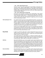
RAM Page Z Select Register –
RAMPZ
The RAMPZ register is normally used to select which 64K RAM page is accessed by the
Z pointer. As the ATmega103(L) does not support more than 64K of SRAM memory,
this register is used only to select which page in the program memory is accessed when
the ELPM instruction is used. The different settings of the RAMPZ0 bit have the follow-
ing effects:
Note that LPM is not affected by the RAMPZ setting.
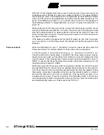
MCU Control Register –
MCUCR
The MCU Control Register contains control bits for general MCU functions.
• Bit 7 – SRE: External SRAM Enable
When the SRE bit is set (one), the external data SRAM is enabled, and the pin functions
AD0 - 7 (Port A), and A8 - 15 (Port C) are activated as the alternate pin functions. Then
the SRE bit overrides any pin direction settings in the respective data direction registers.
When the SRE bit is cleared (zero), the external data SRAM is disabled and the normal
pin and data direction settings are used.
• Bit 6 – SRW: External SRAM Wait State
When the SRW bit is set (one), a one-cycle wait state is inserted in the external data
SRAM access cycle. When the SRW bit is cleared (zero), the external data SRAM
access is executed with a three-cycle scheme. See Figure 51 on page 80 and Figure 52
on page 80.
• Bit 5 – SE: Sleep Enable
The SE bit must be set (one) to make the MCU enter the Sleep Mode when the SLEEP
instruction is executed. To avoid the MCU entering the Sleep Mode unless it is the pro-
grammer’s purpose, it is recommended to set the Sleep Enable (SE) bit just before the
execution of the SLEEP instruction.
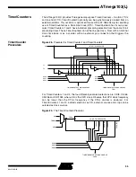
• Bits 4, 3 – SM1/SM0: Sleep Mode Select Bits 1 and 0
This bit selects between the three available sleep modes as shown in Table 3.
Bit
7
6
5
4
3
2
1
0
$3B ($5B)
–
–
–
–
–
–
–
RAMPZ0
RAMPZ
Read/Write
R
R
R
R
R
R
R
R/W
Initial Value
0
0
0
0
0
0
0
0
RAMPZ0 = 0:
Program memory address $0000 - $7FFF (lower 64K bytes) is
accessed by ELPM
RAMPZ0 = 1:
Program memory address $8000 - $FFFF (higher 64K bytes) is
accessed by ELPM
Bit
7
6
5
4
3
2
1
0
$35 ($55)
SRE
SRW
SE
SM1
SM0
–
–
–
MCUCR
Read/Write
R/W
R/W
R/W
R/W
R/W
R
R
R
Initial Value
0
0
0
0
0
0
0
0
Table 3.
Sleep Mode Select
SM1
SM0
Sleep Mode
0
0
Idle Mode
0
1
Reserved
1
0
Power-down
1
1
Power-save


