23
ATmega103(L)
0945G–09/01
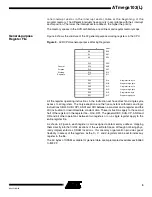
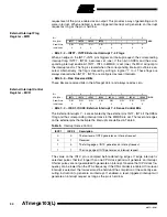
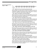
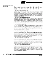
• Bits 2..0 – Res: Reserved Bits
These bits are reserved bits in the ATmega103(L) and always read as zero.
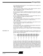
XTAL Divide Control Register
– XDIV
The XTAL Divide Control Register is used to divide the XTAL clock frequency by a num-
ber in the range 1 - 129. This feature can be used to decrease power consumption when
the requirement for processing power is low.
• Bit 7 – XDIVEN: XTAL Divide Enable
When the XDIVEN bit is set (one), the clock frequency of the CPU and all peripherals is
divided by the factor defined by the setting of XDIV6 - XDIV0. This bit can be set and
cleared run-time to vary the clock frequency as suitable to the application.
• Bits 6..0 – XDIV6..XDIV0: XTAL Divide Select Bits 6 - 0
These bits define the division factor that applies when the XDIVEN bit is set (one). If the
value of these bits is denoted
d
, the following formula defines the resulting CPU clock
frequency
f
clk
:
The value of these bits can only be changed when XDIVEN is zero. When XDIVEN is
set to one, the value written simultaneously into XDIV6..XDIV0 is taken as the division
factor. When XDIVEN is cleared to zero, the value written simultaneously into
XDIV6..XDIV0 is rejected. As the divider divides the master clock input to the MCU, the
speed of all peripherals is reduced when a division factor is used.
Reset and Interrupt
Handling
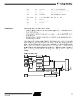
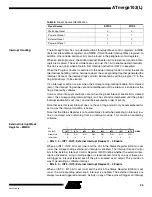
The ATmega103(L) provides 23 different interrupt sources. These interrupts and the
separate reset vector each have a separate program vector in the program memory
space. All interrupts are assigned individual enable bits that must be set (one) together
with the I-bit in the Status Register in order to enable the interrupt.
The lowest addresses in the program memory space are automatically defined as the
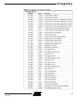
Reset and Interrupt vectors. The complete list of vectors is shown in Table 4. The list
also determines the priority levels of the different interrupts. The lower the address, the
higher the priority level. RESET has the highest priority and next is INT0 (the External
Interrupt Request 0), etc.
Bit
7
6
5
4
3
2
1
0
$3C ($5C)
XDIVEN
XDIV6
XDIV5
XDIV4
XDIV3
XDIV2
XDIV1
XDIV0
XDIV
Read/Write
R/W
R/W
R/W
R/W
R/W
R/W
R/W
R/W
Initial Value
0
0
0
0
0
0
0
0
f
CLK
XTAL
129
d
–
-------------------
=
Table 4.
Reset and Interrupt Vectors
Vector No.
Program
Address
Source
Interrupt Definition
1
$0000
RESET
Hardware Pin, Power-on Reset and Watchdog
Reset
2
$0002
INT0
External Interrupt Request 0
3
$0004
INT1
External Interrupt Request 1
4
$0006
INT2
External Interrupt Request 2
5
$0008
INT3
External Interrupt Request 3
6
$000A
INT4
External Interrupt Request 4

