18
ATmega103(L)
0945G–09/01
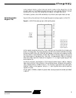
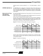
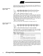
The internal data SRAM access is performed in two System Clock cycles as described
in Figure 22.
Figure 22.
On-chip Data SRAM Access Cycles
See “Interface to External SRAM” on page 79. for a description of the access to the
external SRAM.
I/O Memory
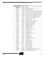
The I/O space definition of the ATmega103(L) is shown in Table 2.
System Clock Ø
WR
RD
Data
Data
Address
Address
T1
T2
T3
T4
Prev. Address
Read
Write
Table 2.
ATmega103(L) I/O Space
I/O Address (SRAM
Address)
Name
Function
$3F ($5F)
SREG
Status REGister
$3E ($5E)
SPH
Stack Pointer High
$3D ($5D)
SPL
Stack Pointer Low
$3C ($5C)
XDIV
XTAL Divide Control Register
$3B ($5B)
RAMPZ
RAM Page Z Select Register
$3A ($5A)
EICR
External Interrupt Control Register
$39 ($59)
EIMSK
External Interrupt MaSK register
$38 ($58)
EIFR
External Interrupt Flag Register
$37 ($57)
TIMSK
Timer/Counter Interrupt MaSK register
$36 ($56)
TIFR
Timer/Counter Interrupt Flag register
$35 ($55)
MCUCR
MCU General Control Register
$34 ($54)
MCUSR
MCU Status Register
$33 ($53)
TCCR0
Timer/Counter0 Control Register
$32 ($52)
TCNT0
Timer/Counter0 (8-bit)
$31 ($51)
OCR0
Timer/Counter0 Output Compare Register
$30 ($50)
ASSR
Asynchronous Mode Status Register
$2F ($4F)
TCCR1A
Timer/Counter1 Control Register A
$2E ($4E)
TCCR1B
Timer/Counter1 Control Register B

