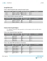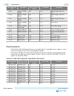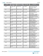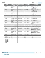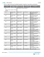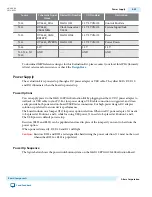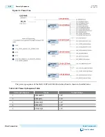
Schematic Signal
Name
Schematic Share
Bus Signal Name
MAX 10 FPGA Pin
Number
I/O Standard
Description
---
GND
---
---
GND
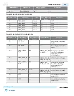
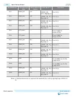
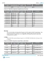
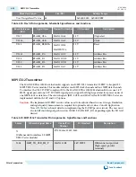
Table 3-15: Pmod B Pin Assignments, Signal Names and Functions
Schematic Signal
Name
Schematic Share
Bus Signal Name
MAX 10 FPGA Pin
Number
I/O Standard
Description
PMODB_D0
PMODB_IO0
C8
3.3 V
In/Out
PMODB_D1
PMODB_IO1
D8
3.3 V
In/Out
PMODB_D2
PMODB_IO2
A3
3.3 V
In/Out
PMODB_D3
PMODB_IO3
A2
3.3 V
In/Out
PMODB_D4
PMODB_IO4
B3
3.3 V
In/Out
PMODB_D5
PMODB_IO5
C2
3.3 V
In/Out
PMODB_D6
PMODB_IO6
B1
3.3 V
In/Out
PMODB_D7
PMODB_IO7
B2
3.3 V
In/Out
---
VCC
---
3.3 V
Power
---
GND
---
---
GND
Memory
This section describes the evaluation board's memory interface support and also their signal names, types,
and connectivity relative to the FPGA. A soft IP memory controller is required as part of the FPGA
design. The memory controller can be a user supplied IP or IP available for purchase from Intel PSG
(formerly Altera) or a partner.
LPDDR2
The MAX 10 FPGA provides full-speed support to a x16 LPDDR2 200-MHz interface by using a 1Gbit x
16 memory.
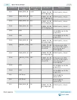
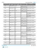
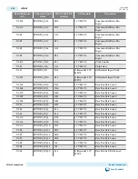
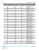
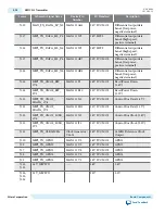
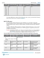
Table 3-16: LPDDR2 Pin Assignments, Signal Names, and Functions
Board Reference
(U2)
Schematic Signal
Name
MAX 10 FPGA Pin
Number
I/O Standard
Description
U2.P3
LPDDR2_CA0
J22
1.2V HSUL
Command/Address Bus
Input
U2.N3
LPDDR2_CA1
J21
1.2V HSUL
Command/Address Bus
Input
U2.M3
LPDDR2_CA2
F22
1.2V HSUL
Command/Address Bus
Input
U2.M2
LPDDR2_CA3
H21
1.2V HSUL
Command/Address Bus
Input
UG-20006
2016.02.29
Memory
3-19
Board Components
Altera Corporation
Send Feedback


