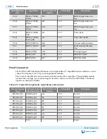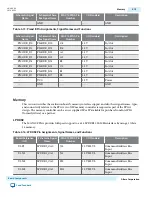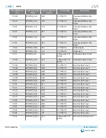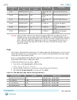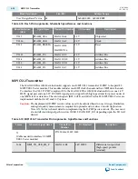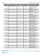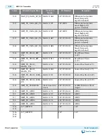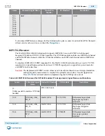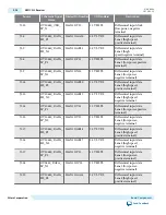
Source
Schematic Signal
Name
Device/Pin Number
I/O Standard
Description
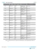
J2.12
OV10640_CLK_
LP_N
MAX 10/T22
1.2V HSTL
Differential input clock
(low power, negative
terminal
J2.8
OV10640_DATA_
HS_P1
MAX 10/AA20
2.5V LVDS
Differential input data
Lane1 (high speed,
positive terminal)
J2.9
OV10640_DATA_
HS_N1
MAX 10/AB21
2.5V LVDS
Differential input data
Lane1 (high
speed,negative terminal)
J2.8
OV10640_DATA_
LP_P1
MAX 10/P21
1.2V HSTL
Differential input data
Lane1 (low power,positive
terminal)
J2.9
OV10640_DATA_
LP_N1
MAX 10/N22
1.2V HSTL
Differential input data
Lane1 (low power,
negative terminal)
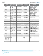
J2.14
OV10640_DATA_
HS_P2
MAX 10/AB20
2.5V LVDS
Differential input data
Lane2 (high speed,
positive terminal)
J2.15
OV10640_DATA_
HS_N2
MAX 10/AB19
2.5V LVDS
Differential input data
Lane2 (high speed,
negative terminal
J2.14
OV10640_DATA_
LP_P2
MAX 10/V21
1.2V HSTL
Differential input data
Lane2 (low power,positive
terminal)
J2.15
OV10640_DATA_
LP_N2
MAX 10/V22
1.2V HSTL
Differential input data
Lane2 (low power,
negative terminal
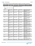
J2.17
OV10640_DATA_
HS_P3
MAX 10/AB18
2.5V LVDS
Differential input data
Lane3 (high speed,
positive terminal)
J2.18
OV10640_DATA_
HS_N3
MAX 10/AB17
2.5V LVDS
Differential input data
Lane3 (high speed,
negative terminal)
J2.17
OV10640_DATA_
LP_P3
MAX 10/Y22
1.2V HSTL
Differential input data
Lane3 (low power,
positive terminal)
J2.18
OV0640_DATA_
LP_N3
MAX 10/W22
1.2V HSTL
Differential input data
Lane3 (low power,
negative terminal)
J2.20
OV10640_DATA_
HS_P4
MAX 10/AA16
2.5V LVDS
Differential input data
Lane4 (high speed,
positive terminal)
3-26
MIPI CSI-2 Receiver
UG-20006
2016.02.29
Altera Corporation
Board Components
Send Feedback

