background image


ACCES I/O Products, Inc. 

MADE IN THE USA 

PCIe-ADIO16-16F Family Manual 


12 

Rev B3d 

FDS models only 

 
In Windows

1

, please consult the various samples (C#, Delphi, and more) to explore how to program the device.  The AIOAIO Software Reference Manual.pdf provides reference material 

covering all AIOAIO Library APIs. A quick reference of the most-applicable functions is provided, below: 
Under certain circumstances the following information might prove useful: 

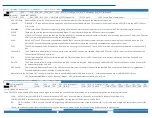
PCI Express Plug-and-Play Data 

BAR[n]  Description 

1:0  DMA Registers 
3:2  I/O Registers 

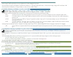
 NOTE ABOUT PERFORMANCE 

The PCI Express bus is capable of very high bandwidth, but the latency per-transaction is roughly the same as all the other busses – it hasn’t improved in decades.  This means you can 
expect to usually see a not-less-than 1MHz transaction rate. Typical rates exceed 3MHz [0.3µs]. 
Unfortunately, modern Operating Systems have introduced a new source of latency, the kernel / userland division. Application code runs in userland, which must transition to the kernel 
in order to perform any hardware operation.  This transition adds quite a lot of latency, which varies between different OSes, motherboards and revisions thereof, etcetera.  A Windows 
XP system can see an additional 7µs per transaction; a modern computer might see 3µs or less.  Any transaction from the kernel itself, however, avoids this additional overhead. 
Real-time operating systems will enable the highest transaction rates possible, all the way up to the hardware limits. 
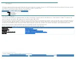
The latest information can always be found on the product page on the website.  Here are some useful links: 
Links to useful downloads 

ACCES web site 

https://accesio.com


Product web page 

accesio.com/PCIe-ADIO16-16F


This manual 

accesio.com/MANUALS/PCIe-ADIO16-16F.pdf


Install Package (Windows XP->10) 

accesio.com/files/packages/PCIe-ADIO16-16F Install.exe


Linux / OSX 

github.com/accesio/APCI


1


In Linux or OSX please refer to the documentation a

github.com/accesio/apci

.


Содержание PCIe-ADIO16-16A

Страница 1: ...Sio com 10623 Roselle Street 800 326 1649 http accesio com PCIe ADIO16 16F San Diego CA 92121 1506 USA sales accesio com MADE IN THE USA 16 ANALOG INPUT 4 ANALOG OUTPUT 16 DIGITAL I O FOR PCI EXPRESS...

Страница 2: ...A D Scan Start mode optimizes inter channel timing High impedance 8 channel input 1 M 32k FIFO plus DMA for efficient robust data streaming 16 Digital I O pins with flexible secondary functions Four 1...

Страница 3: ...0 Ch 0 1 35 ADC IN 1 Ch 0 ADAS3022 1 ADC IN 2 Ch 1 3 37 ADC IN 3 Ch 1 ADC IN 4 Ch 2 5 39 ADC IN 5 Ch 2 ADC IN 6 Ch 3 7 41 ADC IN 7 Ch 3 ADC IN 8 Ch 4 9 43 ADC IN 9 Ch 4 ADC IN 10 Ch 5 11 45 ADC IN 11...

Страница 4: ...CH0 1 0 Advanced Sequence Acquires Channel 0 using the gain selected via 18 bits 2 0 Conversion starts will automatically cycle through the channels from CH0 through INx2 0 and each channel is acquir...

Страница 5: ...ol bit and status 4 W DAC Control DAC LTC2664 Command Register bits 8 W DAC Waveform Divisor DAC Waveform Points second divisor Base Clock DAC Waveform Rate this register C R ADC Base Clock Frequency...

Страница 6: ...to their power on reset state see each ADC Register for more details RST BOARD Writing a 1 will reset the entire device to its power on reset state All RST bits are command bits a 1 causes the reset t...

Страница 7: ...llion 125MHz but for broadest compatibility software should always read this register during init and always use the read value when calculating what if any divisor to write to the ADC Rate Divisor re...

Страница 8: ...19 D18 D17 D16 D15 D14 D13 D12 D11 D10 D9 D8 D7 D6 D5 D4 D3 D2 D1 D0 Name RSV AIN 15 GAIN2 0 RSV AIN 14 GAIN2 0 RSV AIN 13 GAIN2 0 RSV AIN 12 GAIN2 0 RSV AIN 11 GAIN2 0 RSV AIN 10 GAIN2 0 RSV AIN 9 GA...

Страница 9: ...rol 38 for important information about the Channel bits re Differential operation Diff SET indicates the paired ADC Counts were sampled in Differential mode Refer to ADC Control 38 for important infor...

Страница 10: ...5 D9 D8 D7 D6 D5 D4 D3 D2 D1 D0 Name WDG UNUSED EXT1 EXT0 LDAC FOF FAF DTO DDONE ADCSTART ADCTRIG UNUSED enEXT1 enEXT0 enLDAC enFOF enFAF enDTO enDDONE enADCSTART enADCTRIG Read IRQ Status to determin...

Страница 11: ...as a configurable active edge rising or falling SET the corresponding edgeXXX bit to select rising edge CLEAR the bit for falling edge IOGx SET each IOGx bit to configure the digital I O bits in the a...

Страница 12: ...ave introduced a new source of latency the kernel userland division Application code runs in userland which must transition to the kernel in order to perform any hardware operation This transition add...

Страница 13: ...all applicable EM interference and emission standards However as they are intended for use installed on motherboards and inside the chassis of industrial PCs important care in the selection of PC and...

Страница 14: ...and invoiced COVERAGE FIRST THREE YEARS Returned unit part will be repaired and or replaced at ACCES option with no charge for labor or parts not excluded by warranty Warranty commences with equipmen...

Отзывы: