background image


ACCES I/O Products, Inc. 

MADE IN THE USA 

PCIe-ADIO16-16F Family Manual 


Rev B3d 

All these registers can be operated from any operating system using any programming language, using either no driver at all (kernel mode, Linux ioperm(3), DOS, etc.) or using one of the 
ACCES provided drivers (AIOWDM [for Windows], APCI [for Linux & OSX]), or using any 3

rd

 party APIs such as provided with Real-Time OSes.  Addresses not explicitly documented are 

reserved and should not be accessed. 

REGISTER DETAILS 

Register bits labeled UNUSED or RSV are reserved and should be cleared to zero in all write operations and ignored in all read operations. 

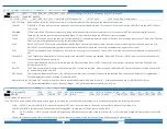
Resets and Power, 0 of 64-bit Memory BAR[2+3] Read/Write 32-bits only 

bit  D31 THROUGH D7 

D6 

D5 

D4 

D3 

D2 

D1 

D0 

Name  UNUSED 

RST FIFO 

RST DIO 

UNUSED 

RST DAC 

PD ADC 

RST ADC 

RST BOARD 

RST FIFO:  

Writing with bit D6 set will reset the ADC FIFO, returning it to the power-on / reset state:  emptying the FIFO by throwing away the contents. 

RST DIO:  

Writing with bit D5 set will reset the Digital I/O circuits to their power-on / reset state: returning all I/O Groups to input mode and disabling secondary 
functions. 

RST DAC: 

Writing with bit D3 set will reset the Analog Output circuits to their power-on / reset state: ±10V range on all DAC outputs with 0V on each output. 

PD ADC: 

Writing a 1 will power the ADAS3022 down.  Write a 0 to power the ADAS3022 back up.  Only this bit does not auto-clear to zero on write. 

RST ADC:  

Writing a 1 will reset the Analog Input circuits to their power-on / reset state: see each ADC Register for more details 

RST BOARD:  

Writing a 1 will reset the entire device to its power-on / reset state. 

 
All RST bits are “command” bits: a 1 causes the reset to occur, and the reset clears the 1. 

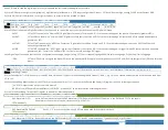
DAC Control, 4 of 32-bit Memory BAR[1]Read/Write 32-bits only 

bit  D31 

D30 

D29 

D28 

D27-D24  D23 through 

D20 

D19 through D16 

D15 through D0 

Name  DAC SPI busy  unused  DAC Waveform 

Running 

DAC FHE  unused 

C3  C2  C1  C0  A3  A2  A1  A0 

16-bit DAC Counts (0-FFFF) 

Bits 31, 29, and 28 are read-only.  Bits 29 and 28 only exist on the FDS models. 

Bit 31:   If set the DAC SPI bus is busy; avoid writing to +4 while this bit is set 
Bit 29:   If set the DAC Waveform Playback is in-process 
Bit 28:   If set the DAC Waveform FIFO is less than half full 
Please refer to the LTC2664 Data Sheet for details regarding bits D23-D0 

Consult the AIOAIO Software Reference, or our sample programs’ source, to avoid the hassle: 

DAC_SetRange1(iBoard, iChannel, iRange); 
DAC_OutputV(iBoard, iChannel, double Voltage); 


DAC Waveform Rate Divisor, 8 of 32-bit Memory BAR[1]Read/Write 32-bits only 

Write a 32-bit divisor to control the speed at which DAC Waveform playback occurs (Points per second).  Each timeout of this clock causes the DACs to simultaneously output the 
last loaded values; the FPGA then writes the next Point from the DAC Waveform FIFO to the DAC chip.  A Point consists of 1, 2, 3, or 4 DAC control words as specified at +54. 

DAC Waveform Rate Divisor = integer(Base Clock ÷ Target DAC Waveform Output Rate) 
Actual DAC Waveform playback (Points/second) Rate (Hz) = Base Clock ÷ DAC Waveform Rate Divisor 


FDS models only 

Base Clock, C of 32-bit Memory BAR[1]Read Only 32-bits only 

Содержание PCIe-ADIO16-16A

Страница 1: ...Sio com 10623 Roselle Street 800 326 1649 http accesio com PCIe ADIO16 16F San Diego CA 92121 1506 USA sales accesio com MADE IN THE USA 16 ANALOG INPUT 4 ANALOG OUTPUT 16 DIGITAL I O FOR PCI EXPRESS...

Страница 2: ...A D Scan Start mode optimizes inter channel timing High impedance 8 channel input 1 M 32k FIFO plus DMA for efficient robust data streaming 16 Digital I O pins with flexible secondary functions Four 1...

Страница 3: ...0 Ch 0 1 35 ADC IN 1 Ch 0 ADAS3022 1 ADC IN 2 Ch 1 3 37 ADC IN 3 Ch 1 ADC IN 4 Ch 2 5 39 ADC IN 5 Ch 2 ADC IN 6 Ch 3 7 41 ADC IN 7 Ch 3 ADC IN 8 Ch 4 9 43 ADC IN 9 Ch 4 ADC IN 10 Ch 5 11 45 ADC IN 11...

Страница 4: ...CH0 1 0 Advanced Sequence Acquires Channel 0 using the gain selected via 18 bits 2 0 Conversion starts will automatically cycle through the channels from CH0 through INx2 0 and each channel is acquir...

Страница 5: ...ol bit and status 4 W DAC Control DAC LTC2664 Command Register bits 8 W DAC Waveform Divisor DAC Waveform Points second divisor Base Clock DAC Waveform Rate this register C R ADC Base Clock Frequency...

Страница 6: ...to their power on reset state see each ADC Register for more details RST BOARD Writing a 1 will reset the entire device to its power on reset state All RST bits are command bits a 1 causes the reset t...

Страница 7: ...llion 125MHz but for broadest compatibility software should always read this register during init and always use the read value when calculating what if any divisor to write to the ADC Rate Divisor re...

Страница 8: ...19 D18 D17 D16 D15 D14 D13 D12 D11 D10 D9 D8 D7 D6 D5 D4 D3 D2 D1 D0 Name RSV AIN 15 GAIN2 0 RSV AIN 14 GAIN2 0 RSV AIN 13 GAIN2 0 RSV AIN 12 GAIN2 0 RSV AIN 11 GAIN2 0 RSV AIN 10 GAIN2 0 RSV AIN 9 GA...

Страница 9: ...rol 38 for important information about the Channel bits re Differential operation Diff SET indicates the paired ADC Counts were sampled in Differential mode Refer to ADC Control 38 for important infor...

Страница 10: ...5 D9 D8 D7 D6 D5 D4 D3 D2 D1 D0 Name WDG UNUSED EXT1 EXT0 LDAC FOF FAF DTO DDONE ADCSTART ADCTRIG UNUSED enEXT1 enEXT0 enLDAC enFOF enFAF enDTO enDDONE enADCSTART enADCTRIG Read IRQ Status to determin...

Страница 11: ...as a configurable active edge rising or falling SET the corresponding edgeXXX bit to select rising edge CLEAR the bit for falling edge IOGx SET each IOGx bit to configure the digital I O bits in the a...

Страница 12: ...ave introduced a new source of latency the kernel userland division Application code runs in userland which must transition to the kernel in order to perform any hardware operation This transition add...

Страница 13: ...all applicable EM interference and emission standards However as they are intended for use installed on motherboards and inside the chassis of industrial PCs important care in the selection of PC and...

Страница 14: ...and invoiced COVERAGE FIRST THREE YEARS Returned unit part will be repaired and or replaced at ACCES option with no charge for labor or parts not excluded by warranty Warranty commences with equipmen...

Отзывы: