ACCES I/O Products, Inc.
MADE IN THE USA
PCIe-ADIO16-16F Family Manual
8
Rev B3d
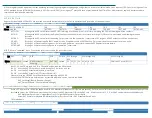
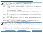
ADC Advanced Sequencer Gain Control, 18 of 32-bit Memory BAR[1]Read/Write 32-bits only
bit D31 D30 D29 D28 D27 D26 D25 D24 D23 D22 D21 D20 D19 D18 D17 D16 D15 D14 D13 D12 D11 D10 D9 D8 D7 D6 D5 D4 D3 D2 D1 D0
Name RSV AIN 7 GAIN2:0 RSV AIN 6 GAIN2:0 RSV AIN 5 GAIN2:0 RSV AIN 4 GAIN2:0 RSV AIN 3 GAIN2:0 RSV AIN 2 GAIN2:0 RSV AIN 1 GAIN2:0 RSV AIN 0 GAIN2:0
Each nybble configures the gain of the corresponding Analog Input channel ONLY when the ADC is running in Advanced Sequenced mode.
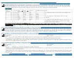
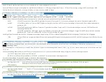
Table 1 - Gain Codes
GAIN2:0
“gain code”
D2 D1 D0 Range
Volts
per pin
1
Range
V p-p, MAX
1
µV
/
Count
Differential rejection
V
Notes
0
0
0
0
±12
49.15
750
The voltage range is shown as recommended max voltage per input
pin.
The recommendation is slightly narrower than max to allow
calibration.
The voltages that can be
measured,
between the + input and the – or
COMMON inputs, are double: the ±12V range will return voltages
b24V and -24V, or “48V p-p”.
1
0
0
1
±5
20.48
312.5
±5.12
2
0
1
0
±2.5
10.24
156.3
±7.68
3
0
1
1
±1.25
5.12
75.13
±8.96
4
1
0
0
±0.625
2.56
39.06
±9.60
5
1
0
1
±0.3125
1.28
19.53
±9.92
7
1
1
1
±10
40.96
625
Gain code 6 (110) is reserved and will result in undefined behavior
Note 1: ApV to IN+ and -V to IN- (or ADC COMMON) results in 2×V span; reversing the voltage polarity results in another 2×V span, for a total Peak-to-Peak measurement
capability of 4×V p-p
ADC Advanced Sequencer Gain Control #2, 1C of 32-bit Memory BAR[1]Read/Write 32-bits only
bit D31 D30 D29 D28 D27 D26 D25 D24 D23 D22 D21 D20 D19 D18 D17 D16 D15 D14 D13 D12 D11 D10 D9 D8 D7 D6 D5 D4 D3 D2 D1 D0
Name RSV AIN 15 GAIN2:0 RSV AIN 14 GAIN2:0 RSV AIN 13 GAIN2:0 RSV AIN 12 GAIN2:0 RSV AIN 11 GAIN2:0 RSV AIN 10 GAIN2:0 RSV AIN 9 GAIN2:0 RSV AIN 8 GAIN2:0
Each nybble configures the gain of the corresponding Analog Input channel ONLY when the ADC is running in Advanced Sequenced mode.
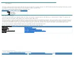
ADC FIFO Almost Full IRQ Threshold, 20 of 32-bit Memory BAR[1]Read/Write 32-bits only
bit D31 through D12
D11 through D0
Name UNUSED
FAF
FAF:
Write any 12-bit value (0..4095) to set the amount of entries in the ADC FIFO allowed to accumulate before a FIFO Almost Full IRQ is fired.
In Software ADC Start mode (ADC Rate Divisor (+10) cleared to zero) the FIFO is 32-bits wide, able to hold up to 4095 conversion results (+statuses).
In all other ADC Start Modes the ADC FIFO is 64-bits wide, holds two ADC Conversions (+statuses) per FIFO entry and the FIFO thus holds 8190 conversion/status pairs. Refer to
the ADC FIFO (+30) register description for more details.
ADC FIFO Count, 28 of 32-bit Memory BAR[1]Read-Only 32-bits only
bit D31 through D12
D11 through D0
Name UNUSED
FIFO Count
FIFO Count:
Read FIFO Count to determine how many entries the ADC FIFO contains.
In Software ADC Start Mode (ADC Rate Divisor (+10) cleared to zero) the FIFO Count determines how many ADC Conversions (+statuses) are held in the FIFO. Read the ADC FIFO
this many times to gather the acquired ADC Data.
In all other modes the FIFO Count reports the number of
pairs
of ADC Conversions are available in the FIFO. Were you to read the data from the ADC FIFO (+30) you would read
two 32-bit values per FIFO Count to gather the acquired data. However, in these modes it is generally best to let DMA transfer the FIFO data, which is performed at the native
64-bit FIFO width.

