ACCES I/O Products, Inc.
MADE IN THE USA
PCIe-ADIO16-16F Family Manual
10
Rev B3d
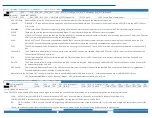
COM: If COM is set then each conversion will be the measurement between the IN+ pin and COMMON (single-ended or pseudo-differential mode). If COM is clear then
differential mode is set, and each conversion will be the measurement between the IN+ and IN- pins.
Gain2:0: If BASIC or non-sequenced mode is configured via the SEQ1:0 bits then Gain2:0 selects the gain to be used for the conversion(s) commanded. If advanced sequence
mode is configured then these bits are ignored (bits 2:0 at +18 take precedence in advanced sequencer mode)
/MUX: All users should set this bit to “1” unless otherwise instructed by the factory. If MUX is clear (0) then the conversion will be from the auxiliary mux inputs (in non-
sequencer mode) or the sequence will include the aux input (sequencer modes). Not recommended.
SEQ1:0: Use “00” for non-sequenced mode and “10” for advanced sequencer mode. “11” sets basic sequencer mode, and “01” updates the basic sequence-in-progress. Not
recommended.
/TEMP: If TEMP is clear (0) then the conversion will be from the onboard temperature reference (in non-sequencer mode) or the sequence will include the temperature input
(sequencer modes). Not recommended. Most users should set this bit to 1.
CMS:
Must be set if conversion will occur slower than 1kHz. Must be clear if conversions will occur faster than 900kHz.
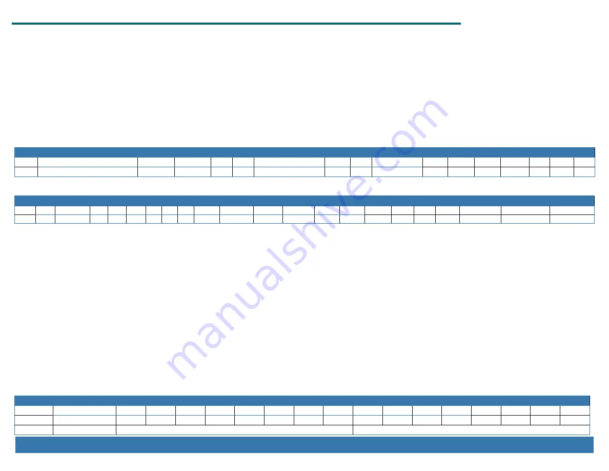
ADC Control #2, 3C of 32-bit Memory BAR[1]Read/Write 32-bits only
bit D31 through D19
D18
D17
D16 D15 D14 through D12
D11
D10 D9 through D7 D6
D5
D4
D3
D2
D1
D0
Name UNUSED
RSV
CONFIG
RSV RSV IN
x
2:0
COM RSV Gain2:0
/MUX SEQ1 SEQ0 /TEMP RSV CMS RSV
Controls ADAS #1, channels 8-15. Refer to +38, ADC Control #1, for details.
IRQ Enable/Clear and Status, 40 of 64-bit Memory BAR[2+3] Read/Write 32-bits only
bit D31 D30 … D25 D24 D23 D22 D21 D20 D19 D18
D17
D16
D15 … D9 D8
D7
D6
D5
D4
D3
D2
D1
D0
Name WDG UNUSED
EXT1 EXT0 LDAC FOF FAF DTO DDONE ADCSTART ADCTRIG UNUSED enEXT1 enEXT0 enLDAC enFOF enFAF enDTO enDDONE
enADCSTART
enADCTRIG
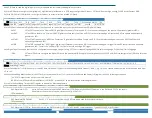
Read IRQ Status to determine which/if any IRQs have fired (D23…D16), if the Watchdog has Barked (D31), and which IRQs are enabled (D7…D0):
WDG:
If WDG is SET then the Watchdog Timer has Barked (timed out). Refer to Watchdog Control (+4C) for details on using the Watchdog Timer feature.
EXT
n
:
If EXT
n
is SET then an IRQ has been fired from the DIO
n
Secondary Function “External IRQ
n
”. Refer to DIO Control (+48) for details on DIO Secondary Functions.
LDAC:
If LDAC is SET then an IRQ has been fired from the DIO 1 Secondary Function “LDAC”. Refer to DIO Control (+48) for details on DIO Secondary Functions.
FOF:
If FOF is SET then an IRQ has been fired because the ADC FIFO has Overrun: More data was acquired than fit in the ADC FIFO.
FAF:
If FAF is SET then an IRQ has been fired because the ADC FIFO Count (+28) has reached the configured FIFO Almost Full IRQ Threshold (+20).
DTO:
If DTO is SET then a DMA Timeout IRQ has been fired.
DDONE:
If DDONE is SET then a DMA Done IRQ has been fired.
ADCSTART: If ADCSTART is SET then an IRQ has been fired from the DIO 0 Secondary Function “ADCSTART”. Refer to DIO Control (+48) for details on DIO Secondary Functions.
ADCTRIG:
If ADCTRIG is SET then an IRQ has been fired from the DIO 0 Secondary Function “ADCTRIG”. Refer to DIO Control (+48) for details on DIO Secondary Functions.
Bits D8 through D0 indicate if the corresponding IRQ has been enabled.
Write IRQ Status bits SET to clear the latched IRQ Status bit(s). Typically, code will read +40 and write the value to +40 to clear all detected IRQs and leave the IRQ enables unchanged.
Write IRQ Enable bits SET to enable corresponding IRQ sources.
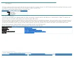
DIO Data, 44 of 64-bit Memory BAR[2+3] Read/Write 32-bits only
bit D31 through D16 D15
D14
D13
D12
D11
D10
D9
D8
D7
D6
D5
D4
D3
D2
D1
D0
Name UNUSED
DIO15 DIO14 DIO13 DIO12 DIO11 DIO10 DIO9
DIO8
DIO7
DIO6
DIO5
DIO4
DIO3
DIO2
DIO1
DIO0
I/O GROUP
I/O Group 1
I/O Group 0

