ACCES I/O Products, Inc.
MADE IN THE USA
PCIe-ADIO16-16F Family Manual
13
Rev B3d
C
HAPTER
8:
S
PECIFICATIONS
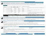
PC Interface
PCI Express Card
Half-height/ length with latching I/O connector
Analog Inputs
ADC Type
Successive approximation
Resolution
16-bit differential bipolar ADC
Sampling rate
2 Msps aggregate (1MHz per simultaneous ADC)
Number of channels
16+0, 8+4, or 0+8 (SINGLE-ENDED + DIFFERENTIAL)
(software selectable)
Differential Bipolar
Ranges (V)
±12, ±10, ±5, ±2.5, ±1.25, ±0.625, ±0.3125V
with 0, 0, ±5.12, ±7.68, ±8.96, ±9.60, ±9.92V common
mode rejection, respectively
4-20mA or 10-50mA
Factory options
Int Nonlinearity Error ±0.6 LSB to ±1.5 LSB depending on gain
No Missing Codes
16 bits
Input Impedance
>500MΩ
A/D Start Sources
Software Start, Timer Start, External Start, Externally
Triggered Timer Start
A/D Start Types
Single Channel or Scan
Overvoltage
Protection
Current limiting through 2 k
Ω
Crosstalk
-120dB @ 10kHz
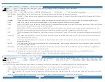
Analog Outputs
Number
4
Type:
Single-ended
Resolution:
16-bit
Bipolar Ranges:
±2.5V, ±5V, ±10V
Unipolar Ranges:
0-5V, 0-10V, 4-20mA
Settling Time
20us typical, +/-10V (+/-1LSB at 16 bits)
Output Current
max ±10mA per channel
Digital Input / Output Interface
Digital Bits
16, in two 8-bit direction controllable I/O Groups
Performance
1 µs per transaction max
(~3.5µs in non-kernel, Windows)
Digital Inputs
Logic High
Logic Low
2.0V to VCCIO (3.3VDC, 5VDC tolerant)
0V to 0.8V
Digital Outputs
Logic High
Logic Low
2.0V (min) 24mA source
0.55V (max) 24mA sink
Environmental
Temperature
Operating 0°C to +70°C
-40°C to +85°C (-T option)
Storage
-40°C to +105°C
Humidity
5% to 95% RH, non-condensing
Dimensions
Length
92.96mm (3.66“)
Height
56.134mm (2.21”)
Weight
53.0 grams
Power
Power required
+3.3VDC @ 400mA (idle) 495mA (full load)
I/O Interface Connectors
On card
68-Pin SCSI Female, with latches
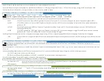
Model Options
-T
Extended Temperature Operation (-40° to +85°C)
-I / -ID
4-20mA inputs (Singled-ended / Differential)
-PD
Pull downs on digital bits
-Sxx
Special configurations (10-50mA DACs or ADCs, input
voltage dividers, conformal coating, etc.)
C
HAPTER
9:
C
ERTIFICATIONS
CE & FCC
These devices are designed to meet all applicable EM interference
and emission standards. However, as they are intended for use
installed on motherboards, and inside the chassis of industrial
PCs, important care in the selection of PC and chassis is important
to achieve compliance for the computer as a whole.
UL & TUV
Neither DC voltages above 3.3V, nor AC voltages of any kind, are
consumed or produced during normal operation of this device.
This product is therefore exempt from any related safety
standards. Use it with confidence!
ROHS / LEAD-FREE STATEMENT
All models are produced in compliance with RoHS and various
other lead-free initiatives.
WARNING
A SINGLE STATIC DISCHARGE CAN DAMAGE YOUR CARD
AND CAUSE PREMATURE FAILURE! PLEASE FOLLOW ALL
REASONABLE PRECAUTIONS TO PREVENT A STATIC
DISCHARGE SUCH AS GROUNDING YOURSELF BY TOUCHING
ANY GROUNDED SURFACE PRIOR TO TOUCHING THE CARD.
ALWAYS CONNECT AND DISCONNECT YOUR FIELD CABLING
WITH THE COMPUTER POWER OFF. ALWAYS TURN
COMPUTER POWER OFF BEFORE INSTALLING A CARD.
CONNECTING AND DISCONNECTING CABLES, OR
INSTALLING CARDS, INTO A SYSTEM WITH THE COMPUTER
OR FIELD POWER ON MAY CAUSE DAMAGE TO THE I/O
CARD AND WILL VOID ALL WARRANTIES, IMPLIED OR
EXPRESSED.
WARRANTY
Prior to shipment, ACCES equipment is thoroughly inspected and
tested to applicable specifications. However, should equipment
failure occur, ACCES assures its customers that prompt service
and support will be available. All equipment originally
manufactured by ACCES which is found to be defective will be
repaired or replaced subject to the following considerations:
GENERAL
Under this Warranty, liability of ACCES is limited to replacing,
repairing or issuing credit (at ACCES discretion) for any products
which are proved to be defective during the warranty period. In
no case is ACCES liable for consequential or special damage
arriving from use or misuse of our product. The customer is
responsible for all charges caused by modifications or additions to
ACCES equipment not approved in writing by ACCES or, if in
ACCES opinion the equipment has been subjected to abnormal
use. "Abnormal use" for purposes of this warranty is defined as
any use to which the equipment is exposed other than that use
specified or intended as evidenced by purchase or sales

