ACCES I/O Products, Inc.
MADE IN THE USA
PCIe-ADIO16-16F Family Manual
5
Rev B3d
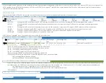
SINGLE AND SCAN START MODES
Each ADC Start Event can be configured to start either a Scan of channels or a single channel conversion.
Single Start Mode: Writing to +38 with bit 18 clear (to 0) selects “Single Start Mode”. Each ADC Start Event, regardless of source, will acquire one channel. No subsequent conversions
will occur until the next ADC Start Event.
Scan Start Mode: Writing to +38 with bit 18 set (to 1) selects “Scan Start Mode”. Each ADC Start Event will acquire the full configured sequence of channels, starting with CH0 and
proceeding through INx2:0, then no further data will be acquired until a subsequent ADC Start Event. The channels within this “scan” of data are acquired at the rate selected via +14. Bit
18 is ignored (assumed zero) if non-Sequenced mode is set (SEQ1:0=00) or if INx2:0==0.
Software Pro Tips:
•
Use our API. Avoid accessing the card registers unless you really know you need to. Contact us for any questions, we’re here to help.
•
Always use Advanced Sequencer Mode.
•
Always prefer Scan Start Mode unless you have unusual timing needs.
•
Set the periodic rate at +10, set the inside-scan channel rate at +14, configure External Trigger if you are using it, configure the per-channel gains at +18 and +1C, then write to
+3C then +38 to Start or Arm (in Software or ADC Trigger modes, respectively) the Periodic Scans.
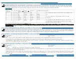
Register Overview
Register
Offset [hex]
Read
/Write
Register Name
Register Description
Note: All registers 4-68 must be accessed as 32-bits. Only +0 and +1 are 8-bits
+0 RW
Resets and Power
Board and Feature Reset command bits and ADC Power-Down control bit and status
+4 W
DAC Control
DAC (LTC2664) Command Register bits
+8* W
DAC Waveform Divisor
DAC Waveform Points/second divisor = Base Clock / DAC Waveform Rate (this register)
+C R
ADC Base Clock
Frequency of the ADC Sequencer Base Clock (Hz) used to calculate the ADC Rate Divisor for desired conversion rates
+10 W/R
ADC Rate Divisor
ADC Start Rate = ADC Base Clock / ADC Rate Divisor (this register)
+14 W/R
ADC Rate Divisor #2
Controls rate of channels inside each scan when running in scan-start mode
+18 W/R
ADC #0 ADV Sequence Gain Each nybble controls the gain code (input range) of the respective ADC channel (0-7)
+1C W/R
ADC #1 ADV Sequence Gain Each nybble controls the gain code (input range) of the respective ADC channel (8-15)
+20 W/R
ADC FAF Threshold
ADC FIFO Almost Full Threshold, can be enabled to generate IRQs when the threshold amount of ADC data is available in the FIFO
+28 R
ADC FIFO Count
ADC FIFO Depth: read to determine how much data is available in the FIFO
+30 R
ADC FIFO Data
ADC FIFO
+38 W/R
ADC #0 Control
ADAS3022 #0 and ADC Control bits
+3C W/R
ADC #1 Control
ADAS3022 #1
+40 W/R
IRQ Enable / Status
IRQ Latch Clear bits and IRQ Enable Control bits / IRQ Latch Status and IRQ Enable Status
+44 W/R
DIO Data
16-bits of DIO Data
+48 W/R
DIO Control
Digital Secondary Function enable bits and direction control for each I/O Group
+50* RW
DAC Waveform FIFO
Write DAC Control values here to load into the DAC Waveform FIFO; read to determine how many samples are in the FIFO
+54* W
DAC Waveform DACs/Point Write 1, 2, 3, or 4 to configure how many samples are written from the DAC Waveform FIFO to the DACs on each DAC Waveform tick
+58* R
DAC Waveform FIFO Size
Size of the DAC Waveform FIFO (+50) in number of 32-bit DAC control values (0x2000 is typical)
+68 R
Revision
FPGA code revision
Note *: These registers are only functional on the FDS models.

