XVME-682 Manual
October, 1989
PIN #
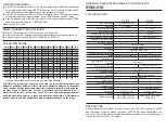
ROW A
SIGNAL
ROW B
SIGNAL
ROW C
SIGNAL
1
I/OCHCK
+5V
N/C
2
SD7
GND
IRQ9
3
SD6
MEMW*
DRQ2
4
SD5
SD8
N/C
5
SD4
SD9
SMEMW*
6
SD3
SD10
SMEMR*
7
SD2
SD11
IOW*
8
SDI
SD12
IOR*
9
SDO
SD13
DACK3*
10
IOCHRDY SD14
DRQ3
11
AEN
SD15
DACK1*
12
SA19
GND
DRQ1
13
SA18
+5V
REFRESH*
14
SA17
MEMCS16*CLK
15
SA16
IOCS16*
IRQ7
16
SAI5
IRQ10
IRQ6
17
SA14
IRQI 1
IRQ5
18
SA13
IRQ12
IRQ4
19
SA I2
IRQ15
IRQ3
20
SA11
IRQ14
DACK2*
3.6 PC/AT INTERFACE CONNECTOR P2/P3
The XVME-682 is made in odd-numbered versions (XVME-682/1 & XVME-682/3) and even-
numbered versions (XVME-682/2 & XVME-682/4). The even-numbered versions of the module
cannot operate with a 32-bit processor sharing the same VMEbus backplane.
This is due to the fact that Row B of the VMEbus P2 connector is bussed to all cards on the
backplane. Because the even-numbered XVME-682 versions use the P2 connector to send AT
signals, they cannot share Row B with a 32-bit processor elsewhere on the backplane.
On all versions, the XT signals travel on the user-defined I/O pins on Rows A & C of the
VMEbus P2 connector.
The pinouts for the XVME-682/2 & XVME-682/4 P2 connectors are as follows:
Table 3-10 PC/AT Interface Connector P2
(XVME-682/2 & XVME-682/4 Only)
3-13
Artisan Technology Group - Quality Instrunnentatio
1 ...
I (888) -SOURCE I
Summary of Contents for XVME-682
Page 5: ......


