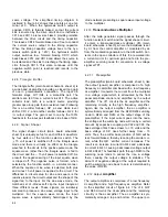
4.1 FUNCTIONAL BLOCK DIAGRAM ANALYSIS
This
section describes the functions of major circuit
elements and their relationship to one another as
shown in figure 4-1, functional block diagram, and
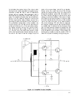
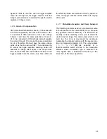
figure 4-2, basic generator and timing diagram.
Paragraph 4.2 provides further descriptions relating
circuit
blocks
to schematics in section 7.
As shown in figure 4-1, the main generator VCG
(Voltage
Control of Generator frequency) summing
amplifier receives inputs from the frequency dial, ver-
nier, FM and PM switches which produce a sum cur-
rent. The PM input is provided with a passive differen-
tiator which produces a voltage proportional to the
rate of change of the instantaneous voltage of the
modulating signal.
The VCG summing amplifier is an inverting amplifier
whose output voltage is used to control a complemen-
tary current source and current sink. For symmetrical
output waveforms, the currents are equal and directly
proportional to the algebraic sum of the VCG inputs.
The diode gate, controlled by the hysteresis switch,
switches either the current source or sink to the timing
capacitor selected by the frequency multiplier con-
trol. When the current source is switched in, the
charge on the capacitor will rise linearly producing
the positive-going triangle slope. Likewise, the current
sink produces the negative-going triangle slope.
The triangle amplifier is a unity gain amplifier whose
output is fed to the hysteresis switch and to the
triangle buffer. The hysteresis switch is a bistable
device operating as a window detector with limit
points set to the triangle peaks. When the hysteresis
switch output is + 2V, the triangle rises to the + 1.25V
limit, and the hysteresis switch goes to - 2V. This
switches currents at the diode gate and the negative-
going triangle slope is started. When the triangle
reaches the - 1.25V limit, the hysteresis switch will
switch back to positive, repeating the process. As
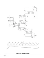
shown in figure 4-2, this repetitive process results in
the simultaneous generation of a square wave and a
triangle wave at the same frequency.
The output frequency is determined by the magnitude
of the capacitor selected by the frequency multiplier
selector and by the magnitude of the currents sup-
plied to and removed from it. Since the currents are
linearly proportional to the sum of VCG inputs, so will
be the output frequency. The capacitance multiplier
provides the bottom four frequency ranges.
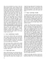
When the variable symmetry control is rotated, it first
reduces the current sink by a factor of 19, making the
negative-going triangle slope 19 times longer than
normal. This results in an unsymmetrical waveform
output and a frequency division by IO. Continued rota-
tion gradually increases the current sink and reduces
the current source in such a way that the period for
the triangle to complete one cycle remains constant.
This action produces continuously variable symmetry
of the output waveforms over a
1:19
to
19:1
range
while frequency remains constant at one-tenth of dial
and multiplier settings.
The inverted square from the hysteresis switch is fed
to the sync amplifier, where it is buffered and con-
verted to a TTL level output, and to the square
amplifier, where (if square or pulse functions are
selected) a buffered square is sent to the signal
shaper for conditioning.
The triangle buffer provides the
1.25 triangle suffi-
cient drive for the signal shaper and presents a small,
constant load on the triangle amplifier.
C
, HYSTERESIS
SWITCH
.
A
Figure 4-2. Basic Generator Block
and Timing Diagram
4-l


