tion amplifies the positive swing of the output, while
the lower mirror portion amplifies the negative swing.
Operation is class AB; that is, there is independent
positive half and negative half amplification, with a
small amount of current flow in both sides near zero
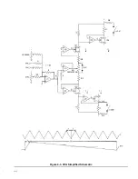
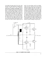
swing. The amplifier schematic has been simplified in
figure 4-4 for the following discussion. Assume that
both the input and the output voltages are zero, then
the voltage at point A should also be zero. Because of
the symmetrical configuration of the amplifier, the
current through Q47 and Q49 will be equal and the
output will remain at zero. If the input goes positive,
the voltage at point A will rise by a certain amount.
This will cause the base voltage of Q47 to
rise
closer
to + 24 volts. Thus, the emitter base junction of Q47
will be less forward biased, thereby reducing its emit-
ter current. The result is that the voltage at point B
I N P U T
U 19/Q37/Q38
r
which is the output voltage, will start to go negative.
Finally, when the output has moved far enough
negative to pull point A back to zero, by pulling current
through the feedback resistor Rfb, the collector cur-
rent of Q47 and Q49 will again be equal and the output
voltage at point B will stabilize. The amount of nega-
tive voltage at the output required to pull point A back
to zero is controlled by the ratio of
to Rin, and this
ratio is the closed loop gain of the output amplifier.
The circuit containing U19, Q37, Q38 is a high gain,
low frequency amplifier used to bias the high frequen-
cy amplifier and to increase the low frequency loop
gain. The high frequency amplifier is isolated from low
frequency signals at the input by capacitance coupl-
ing to the bases of Q47 and Q49. It then employs the
low frequency amplifier to bias the emitter of Q47 to
obtain the required dc stability and high loop gain.
+ 24 Vdc
OUTPUT
- 24
Vdc
Figure 4-4. Simplified Output Amplifier
4-7


