background image

center by an amount determined by the modulation
amplitude.

-Phase Modulation (PM): As in External Modulation.

A m p l i t u d e   o f   m o d u l a t o r

,

,

  f u n c t i o n s

varies phase up to

External Modulation

A BNC feeds an external signal to the modulating cir-

cuits when selected by a front panel modulation tog-
gle switch in the EXT position.

Amplitude Modulation (AM):

External modulating

signals with zero dc component produce suppressed
carrier modulation; i.e., a carrier (at main generator
function output) amplitude of zero. The function out-
put modulated signal has an amplitude sensitivity of
3 volts peak (1.5 Vp into 

per volt peak in. A car-

rier signal level at the function output can be pro-

duced at a sensitivity of 3 Vp (I .5 Vp into 500) per 1 Vp
dc component in. Modulating the dc component mod-

ulates the carrier level. Percent modulation (AM) will
be the ratio of the peak ac to peak dc of the modulating
signal. Input impedance is >2.5

Frequency Modulation (FM) and Sweep: Sensitivity is

20% of frequency range/volt peak. Linear behavior

results only when all instantaneous frequencies call-

ed for fall within the frequency range (2

x

multiplier

to 0.002

x

multiplier). The instantaneous frequency

called for is the multiplier and dial setting altered by
the instantaneous voltage at the modulation input. In-
put impedance is 5

Phase Modulation (PM): Sensitivity is

phase shift/

volt peak. Linear behavior results only when all instan-
taneous transition frequencies called for fall within
the frequency range (2

x

multiplier to 0.002

x

multi-

plier).The  instantaneous frequencies called for will
depend heavily on the modulation frequency. and
waveform. Inoperative at frequency multiplier settings
below 100. Input frequencies roll off at 6 dB/octave
above one half of full range frequency and above

150 kHz.  Input impedance is IO

1.2.1.4,

Frequency Range

0.0002

Hz to 20 MHz in

IO

overlapping ranges with

approximately

1 %

 vernier control.

1.2.1.5

Function Output 

,

and

 selectableandvariable to 30V p-p

(15V  p-p into

and

up to 15 Vp (7.5 Vp

into

All waveforms and dc can supply 150 mA

1-2

peak current and may be attenuated to 60 dB in 20 

dB

steps. An additional 20 dB vernier also controls the
w a v e f o r m   a m p l i t u d e s .

1.2.1.6

Adjustable Waveform Start/Stop Point

Approximately -

 to + 

 to 2 MHz (operative on

sine and triangle waveforms only).

1.2.1.7

DC Output and DC Offset

Selectable through function output

 Controlled

b y   f r o n t   p a n e l   c o n t r o l s   t o   a   m i n i m u m   o f

 14.4 Vdc(   7.2 Vdc into 

 with signal peak plus

offset limited to 

15 Vdc (

 7.5 Vdc into 

 DC off-

set and wave form attenuated proportionately by the
60 dB output attenuator.

1.2.1.8

External Modulation Input

AM: Sensitivity of 3 Vp out/Vp (1.5V into 503). Input

impedance is >2.5
FM: Sensitivity of 20% of frequency range/Vp. Input
impedance is 5
PM :

Sensitivity of

phase shift/VP. Input im-

pedance  is 1O

1.2.1.9

Symmetry

Symmetry of all waveform outputs is continuously ad-

justable from 1 :1 9 to 19:1. Varying symmetry provides
variable duty-cycle pulses, sawtooth ramps and non-
symmetrical sine waves.

N O T E

W h e n   S Y M M E T R Y   c o n t r o l   i s   u s e d ,   i n -

dicated frequency is divided by approx-
ima tely IO.

1.2.1.10 Sync Output (TTL)

TTL level pulse which will drive 10 TTL  loads. Fre-
quency and time symmetry are the same as for func-
tion output.

1.2.1.11 Trlgger and Gate

Input Range: IV p-p to

IOV.

Input Impedance: IO

 33 pF.

Pulse Width: 25 ns minimum.
Repetition Rate: IO MHz maximum.

Adjustable triggered signal start/stop point: approxi-

mately -

 to 

 to 2 MHz.

Summary of Contents for 148A

Page 1: ...NS INFORMATION PRO PRIETARY TO WAVETEK AND IS SOLELY FOR IN STRUMENT OPERATION AND MAINTENANCE THE INFORMATION IN THIS DOCUMENT MAY NOT BE DUPLICATED IN ANY MANNER WITHOUT THE PRIOR APPROVAL IN WRITIN...

Page 2: ...r is quiescent until trig gered by an external signal then generates one cycle at the selected frequency External Gate Same as external trigger except gen erator oscillates at the selected frequency f...

Page 3: ...m Inoperative at frequency multiplier settings below 100 Input frequencies roll off at 6 dB octave above one half of full range frequency and above 150 kHz Input impedance is IO 1 2 1 4 Frequency Rang...

Page 4: ...1 2 2 2 Frequency Range 0 1 Hz to 100 kHz in three 100 1 ranges Sweep 0 2 Hz to 200 kHz 2 x setting and are fixed level 10V p p balanced about ground M and M are fixed level 5 Vp from 0 to 5V 1 2 2 4...

Page 5: ...is quiescent until a proper gate signal is applied at the EXTTRIG IN BNC 13 and then outputs the selected signal for the duration of the gate signal plus the time to complete the last cycle generated...

Page 6: ...red One cycle of waveform for each trigger signal C Gated A burst of waveforms for the dura tion of each gate signal d AM The instantaneous amplitude of the out put signal varies with the instantaneou...

Page 7: ...r gating the generator For manually triggering single cycles the generator mode should be EXT TRIG with no external signal in put at the EXT TRIG IN connector Each time TRIG GER LEVEL is rotated cw th...

Page 8: ...ing decreases and the angle subtended in the nomograph decreases If the MOD AMPLITUDE control is rotated toward MAX the angle subtended would overshoot the OUTPUT FREQUENCY FACTOR range indicating tha...

Page 9: ...red One cycle of waveform for each trigger signal C Gated A burst of waveforms for the dura tion of each gate signal d AM The instantaneous amplitude of the out put signal varies with the instantaneou...

Page 10: ...r gating the generator For manually triggering single cycles the generator mode should be EXT TRIG with no external signal in put at the EXT TRIG IN connector Each time TRIG GER LEVEL is rotated cw th...

Page 11: ...ing decreases and the angle subtended in the nomograph decreases If the MOD AMPLITUDE control is rotated toward MAX the angle subtended would overshoot the OUTPUT FREQUENCY FACTOR range indicating tha...

Page 12: ...per Limit 2 0 x FREQ MULT Lower Limit 0 001 X Upper Limit Nominally the phase of the main generator is shifted ten degrees for each volt of instantaneous modulation signal When the main generator is s...

Page 13: ...and the hysteresis switch goes to 2V This switches currents at the diode gate and the negative going triangle slope is started When the triangle reaches the 1 25V limit the hysteresis switch will swit...

Page 14: ...con tinuous independent of generator mode While the integrating capacitor is being held from charging the start stop diode must sink the current source which has a magnitude variable with VCG in puts...

Page 15: ...across series resistors to the supplies equal to the control voltages The FET currents will be switched at the diode gate into a timing capacitor to produce the triangle waveform 4 2 2 Symmetry Contr...

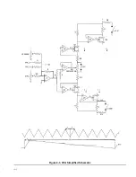
Page 16: ...R 9 VERNIER I R 2 1 R SYMMETRY R R 2 OM R 9 Figure 4 3 VCG Simplified Schematic...

Page 17: ...th output impedance low enough to drive the hyster esis switch and the triangle buffer In series with Q8 is a matched duplicate FET Q9 Q9 has the identical drain current as Q8 and therefore the same g...

Page 18: ...circuit In the positive pulse mode the square wave rather than the triangle wave is fed to the circuit and the 15 volt power is switched off As a result the negative swing of the input square wave is...

Page 19: ...ter current The result is that the voltage at point B I N P U T U 19 Q37 Q38 r which is the output voltage will start to go negative Finally when the output has moved far enough negative to pull point...

Page 20: ...ve than the trigger level is 4 8 clipped by forward biasing CR1 the negative portion is clipped by CR2 While CR1 is on Q1 conducts and Q3 switches off to a TTL low level While CR2 is on Q1 is off and...

Page 21: ...erefore R64 will have the same voltage across it as the drop across CR2 The current leaving Q7 enters the trigger amplifier summing node and becomes a voltage offset equal to the drop across CR2 becau...

Reviews: