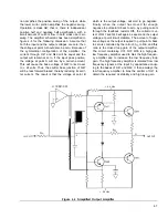
Other circuit components are shown on the main
board schematic, sheet 3. Emitter followers Q46 and
Q48 increase the driving power to the bases of Q47
and Q49. Q51 and Q54 are a harnessed pair sharing
the load through R287 and R291 during the positive
signalswing. Q51 and Q54 are driven by the collector
of Q47. CR40 through CR43 compensate for the
emitter-base junction voltage drops of Q51, Q53, Q54
and Q55 to control idling current, reduce crossover
distortion and prevent thermal runaway. The two
resistor-capacitor networks,
R268/C1 00 and
R278/C101 are emitter bypass circuits to maintain the
high frequency amplifier gain during the transition
time prior to the dc amplifier taking effect. This im-
proves the rise time, since the dc amplifier requires a
few microseconds to respond and stabilize. VR2 and
VR3 are five volt regulators which normally run
saturated to supply the output stage current to the col-
lectors of the output transistors. If the output stage
should demand an abnormal amount of current
through a shorted’transistor or output terminal, the
current through R295 through R298 will generate five
volts of drop. If more current is demanded, the
regulators will simply maintain the five volt drop,
allowing the output collector voltages to collapse,
preventing
excessive power dissipation
in the
amplifier components. The dc offset is fed as a cur-
rent from the front panel control to the output
amplifier summing mode.
4.2.13
Sync Amplifier/Square Amplifier
The side of the hysteresis switch (main board sche-
matic, sheet 2) not used to drive the current switch
has an inverted square signal which is used to drive
an emitter coupled pair, Q16 and Q23. The collector
output of Q23 is biased to provide a TTL level output,
The sync out signal is connected to the front panel
sync out (TTL) BNC with a coaxial cable.
Next to the sync amplifier, a similar emitter coupled
pair, Q57 and Q58, is connected to the same input
and biased to output a bipolar square wave to the
function switch when square or pulse functions are
selected. In other functions, emitter bias is reversed
so that the square function remains confined to the
hysteresis switch area.
4.2.14
Trigger Signal Limiter
Either an external signal or the modulator function are
selected by the generator mode switch (auxiliary
generator schematic) and summed through R50 and
R51 with the trigger level control. That portion of the
trigger signal more positive than the trigger level is
4-8
clipped by forward biasing CR1; the negative portion
is clipped by CR2. While CR1 is on, Q1 conducts and
Q3
switches off to a TTL low level. While CR2 is on, Q1
is off and Q3 saturates to a TTL high level. R57 and
R58 provide hysteresis to ensure a clean square wave
output.
4.2.15
Trigger Logic/Trigger Amplifier
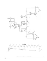
In continuous mode the continuous control line is low
and U13-8 (main board schematic, sheet 2) holds the
trigger flip-flop (U12) cleared. U12-3 is low, which is
sent by emitter follower Q27 to a diode “AND”. A low
is sensed at RI 58, the trigger amplifier inverting input.
The closed loop gain of the trigger amplifier is set by
the ratio of R173 to R158. The trigger amplifier out-
puts a + 1.5 to + 2 Vdc to reverse bias the start/stop
diode CR27 above the most positive charge on the in-
tegrating capacitor.
In trigger mode, both control lines are high, and U13
produces a narrow negative pulse, corresponding to a
high to low transition of the signal limiter output, to
clear U12. In the absence of a trigger stimulus, U12 is
clocked by the negative-going edge of the current
switch square translated by Q26 to TTL levels. U12-3
goes high and the trigger amplifier goes to a low level,
forward biasing CR27 which sinks the VCG current
source away from the integrating capacitor. The
charge level on the integrating capacitor is held at the
voltage drop across CR27 above the trigger amplifier
output. Compensation current enters the trigger
amplifier summing node through R155 to push its out-
put voltage down exactly the same as the drop across
CR27 at a particular magnitude of integrating current.
The 0 Vdc trigger baseline may be modified with R4,
the front panel start/stop control. Whenever a trigger
is received, U13 is cleared and the trigger amplifier
output goes high, allowing the integrating capacitor to
charge. At the positive triangle peak, the hysteresis
switch goes to a negative level and the negative-going
triangle slope is generated. The high-to-low hysteresis
transition clocks U12-3 high, but the negative portion
of the square is also fed into the diode “AND” at
CR20 which holds the trigger amplifier output high un-
til the completion of the negative-going slope of the
triangle. When the hysteresis switch returns to
positive, the trigger amplifier returns to its low output,
and the integrating capacitor charges until CR27 for-
ward biases again. The integrating capacitor is again
held at the trigger baseline level.
In gate mode, the gated control line is low and U13
produces a negative pulse of the same duration as the
signal limiter output. Thus, U12 is held cleared, the


