tion for an external signal to the switches “external”
positions.
The FM and PM switches provide VCG inputs. The AM
switch controls the control amplifier and thus the
transconductance multiplier. When AM is off, the con-
trol amplifier produces a positive dc level giving the
multiplier a fixed gain. With internal AM, the dc com-
ponent from the control amplifier is cut in half, halving
the output amplitude to prevent output clipping when
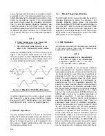
modulating. The selected modulation waveform rides
on the dc. The ac (modulation signal) has a peak value
equal in magnitude to the dc level when the modula-
tion amplitude control is maximum, making the sum of
modulator and carrier signals equal to the maximum
output capability of the output amplifier, and the differ-
ence equal to the zero output level, which is 1 0 0 %
modulation. Then, by varying the modulation signal, a
variable 0 to 100% AM of the carrier (main generator)
signal is produced. With external AM, the dc compo-
nent is switched to 0 Vdc, resulting in zero amplitude
output, and bipolar signal inputs at the EXT MOD IN
connector will produce suppressed carrier (4-quadrant)
modulation.
4.2
CIRCUIT ANALYSIS
4.2.1 VCG Amplifier
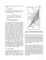
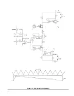
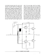
Figure 4-3 is a simplified schematic of the VCG cir-
cuitry. The value of a resistor “R” is 5
and supplies
are
15 Vdc. U1 is connected as a summing
amplifier to sum the VCG inputs. A top of range input
produces 1mA through the feedback resistor resulting
in - 5 Vdc at the output of U1
The negative input of U4 is held at the output level of
U1 by controlling the current through Q2 as a feed-
back. One half the output of U1 is buffered by U3 and
applied to the wiper of the variable symmetry control.
The negative input of U2 is held at 0 Vdc by controlling
the current through Ql as a feedback. As long as the
variable symmetry control is off, the two R/2 resistors
have equal voltage across them and an equal current
through them as through U1 feedback and there is no
current at the output of U3. Since an equal current
exists in the entire resistor string from + to - supply,
the result is a positive control voltage relative to the
negative supply at U6 + input and a negative control
voltage with respect to the positive supply at U5 + in-
put, each of which is proportional to the sum of the in-
puts to U1
Similarly, U5 and U6 establish feedback by regulating
current through FETs, producing a voltage drop
across series resistors to the supplies equal to the
control voltages. The FET currents will be switched at
the diode gate into a timing capacitor to produce the
triangle waveform.
4.2.2
Symmetry Control
Let the source of Q2 be - 5 Vdc, the wiper of the sym-
metry control, - 2.5 Vdc, and the source of Q1, 0 Vdc.
The output of U3 will have no current, each R/2 resis-
tor will have 1 mA, and generator frequency will be at
maximum of the range. Open the symmetry switch
and set the potentiometer to its electrical center. The
output of U3 is still at an equipotential point, but now
the total resistance with 5 Vdc across it has changed
from R to 10R. Thus, current will drop to 100
and
output frequency will drop to one-tenth of range. If the
potentiometer is rotated, current will flow in U3 output
to maintain the wiper at - 2.5 Vdc. When the potentio-
meter is ccw, the wiper is at the positive direction and
the upper R/2 will have 2.5V across it with a current
source of 1 mA. But the lower R/2 is in series with 9R,
which puts 2.5V across 19
x
the normal resistance.
Now the current sink will have one-nineteenth the
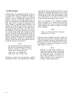
magnitude of the current source. The output waveform
for this condition is shown in figure 4-3. Regardless of
where the symmetry control is rotated, frequency
stays the same (one-tenth of range).
4.2.3
Range Switching
For frequency ranges associated with multiplier posi-
tions of 100 and 1 K, main board schematic, sheet 1,
the value of the current source and current sink setting
resistors R326, R38, R48 and R330 is 5
which pro-
vides integrating current sensitivity of 200
per volt
of external FM input. With the timing capacitors of 1
and 0.1
plus the bulk of the top range timing capa-
citor and the stray capacitance of the multiplier switch,
the generator produces the calibrated output fre-
quency for these ranges. In the top range (multiplier
position of 10M), the current setting resistors are
paralleled with resistors of one-ninth the value, caus-
ing both current sources to run at ten times the usual
current, resulting in 2 mA per volt of external FM input.
When this current is used with the nominal -90 pF
timing capacitor (fixed value plus strays), the top
range of frequencies result. For the next three ranges
down (multiplier positions 1 M, 100K, 10K), the nominal
timing capacitor is the fixed top range capacitor plus
strays (i.e., -90 pF) plus the switched values (11 pF,
9 1 0 pF, 0.01
These result in joint timing
capacitors of 101 pF, 1010 pF and 0.0101
In these
three ranges the positive and negative current
sources are boosted by 1
over the next range down
4-3


