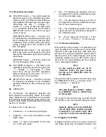
signal at CR24 is held low, and the trigger amplifier
output is held high for the trigger duration. The last
triangle cycle started is completed through the action
explained in trigger mode.
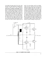
the start/stop diode are matched and carry equal cur-
rents, the trigger baseline will be stable with varying
VCG inputs.
4.2.17
Modulation Generator and Ramp Generator
4.2.16 Baseline
Compensation
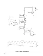
CR2 (main board schematic, sheet
1)
is in series with
the current supplied by the VCG current source. U9-3
is connected to CR2 anode and, since it is a voltage
follower, it will have the same potential at its pin 6.
U1 O-3 is connected to CR2 cathode and will regulate
the current through Q7 to make the same potential at
its pin 2; therefore, R64 will have the same voltage
across it as the drop across CR2. The current leaving
Q7 enters the trigger amplifier summing node, and
becomes a voltage offset equal to the drop across
CR2, because R64 and the feedback resistor for the
trigger amplifier have the same value. Since CR2 and
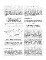
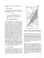
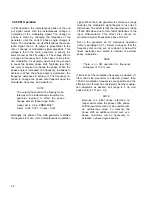
The function generator used as a modulation source
in the instrument is the lntersil 8038 (U2 on the auxil-
iary generator board schematic). It is fitted with an
auxiliary current balancing circuit (U1) to extend its
useful dynamic range. The ramp output which is not
built into the chip is developed by amplitude
modulating the triangle function with the square func-
tion in a balanced modulator (U5). The output signals
(
,
,
,
M )
are selected in a
function selector switch and fed to the modulation
switches where modulation type is selected. The
ramp signals have a fundamental frequency of two
times that of the other waveforms.
4-9


