background image

2.2 Troubleshooting Flowchart   

2 Troubleshooting Procedures  

TECRA M10 Maintenance Manual (960-685) 

 [CONFIDENTIAL] 

2-7 

15.


If a malfunction is detected on the fingerprint sensor, perform the Fingerprint Sensor 
Troubleshooting Procedures in Section 2.18. 

16.


If a malfunction is detected on the Web camera, perform the Web camera 
Troubleshooting Procedures in Section 2.19. 

17.


If a malfunction is detected on the Intel Turbo Memory, perform the Intel Turbo 
Memory Troubleshooting Procedures in Section 2.20. 


Summary of Contents for Tecra M10

Page 1: ... CONFIDENTIAL Toshiba Personal Computer TECRA M10 Maintenance Manual First edition July 2008 TOSHIBA CORPORATION File Number 960 685 ...

Page 2: ...to change without notice Therefore Toshiba assumes no liability for damages incurred directly or indirectly from errors omissions or discrepancies between any succeeding product and this manual Trademarks IBM is a registered trademark and IBM PC is a trademark of International Business Machines Corporation Intel Intel SpeedStep Intel Core Celeron and Centrino are trademarks or registered trademark...

Page 3: ...f a hazard that could result in bodily injury if the safety instruction is not observed CAUTION Caution indicates the existence of a hazard that could result in property damage if the safety instruction is not observed NOTE Note contains general information that relates to your safe maintenance service Improper repair of the computer may result in safety hazards Toshiba requires service technician...

Page 4: ... and resolve FRU problems Chapter 3 Test and Diagnostics describes how to perform test and diagnostic operations for maintenance service Chapter 4 Replacement Procedures describes the removal and replacement of the FRUs Appendices The appendices describe the following Handling the LCD module Board layout Pin assignments Keyboard scan character codes Key layout Wiring diagrams BIOS rewrite procedur...

Page 5: ...ears on the keyboard is printed in boldface type Key operation Some operations require you to simultaneously use two or more keys We identify such operations by the key top symbols separated by a plus sign For example Ctrl Pause Break means you must hold down Ctrl and at the same time press Pause Break If three keys are used hold down the first two and at the same time press the third User input T...

Page 6: ...ardware Overview 1 1 Features 1 1 1 2 System Unit Block Diagram 1 9 1 3 3 5 inch Floppy Disk Drive USB External 1 15 1 4 2 5 inch Hard Disk Drive 1 16 1 5 Optical Drive ODD 1 18 1 6 Keyboard 1 22 1 7 TFT Color Display 1 23 1 8 Power Supply 1 26 1 9 Batteries 1 28 1 10 AC Adaptor 1 31 ...

Page 7: ...Troubleshooting 2 42 2 8 Touch pad Troubleshooting 2 44 2 9 Display Troubleshooting 2 46 2 10 Optical Disk Drive Troubleshooting 2 49 2 11 Modem Troubleshooting 2 51 2 12 LAN Troubleshooting 2 53 2 13 Wireless LAN Troubleshooting 2 54 2 14 Bluetooth Troubleshooting 2 57 2 15 Sound Troubleshooting 2 59 2 16 Bridge media Slot Troubleshooting 2 61 2 17 PCI ExpressCard Slot Troubleshooting 2 62 2 18 F...

Page 8: ... 14 Real Timer Test 3 29 3 15 NDP Test 3 31 3 16 Expansion Test 3 32 3 17 CD ROM DVD ROM Test 3 34 3 18 Error Code and Error Status Names 3 35 3 19 Hard Disk Test Detail Status 3 38 3 20 ONLY ONE TEST 3 40 3 21 Head Cleaning 3 49 3 22 Log Utilities 3 50 3 23 Running Test 3 52 3 24 Floppy Disk Drive Utilities 3 53 3 25 System Configuration 3 58 3 26 Wireless LAN Test Program Atheros 3 60 3 27 Wirel...

Page 9: ...1 SIM board 4 37 4 12 Wireless LAN card 4 39 4 13 3G card 4 41 4 14 Robson card 4 43 4 15 Speaker 4 45 4 16 Cover assembly and Base assembly 4 49 4 17 MDC modem USB board 4 55 4 18 RGB harness RJ45 harness 4 58 4 19 Serial board 4 61 4 20 Microphone harness 15 4 inch model 4 63 4 21 System board 4 64 4 22 GFX board GFX fin 4 69 4 23 CPU CPU fin DC fan 4 72 4 24 PC card unit 4 77 4 25 RTC battery 4...

Page 10: ... 114 4 34 LCD mask 4 117 4 35 Hinge 4 121 4 36 Fluorescent Lamp 4 12 Appendices Appendix A Handling the LCD Module A 1 Appendix B Board Layout B 1 Appendix C Pin Assignments C 1 Appendix D Keyboard Scan Character Codes D 1 Appendix E Key Layout E 1 Appendix F Wiring Diagrams F 1 Appendix G BIOS rewrite Procedures G 1 Appendix H EC KBC rewrite Procedures H 1 Appendix I Reliability I 1 ...

Page 11: ... CONFIDENTIAL Chapter 1 Hardware Overview ...

Page 12: ...1 Hardware Overview 1 ii CONFIDENTIAL TECRA M10 Maintenance Manual 960 685 ...

Page 13: ... 3 3 5 inch Floppy Disk Drive USB External 1 15 1 4 2 5 inch Hard Disk Drive 1 16 1 5 Optical Drive ODD 1 18 1 6 Keyboard 1 22 1 7 TFT Color Display 1 23 1 7 1 LCD Module 1 23 1 7 2 FL Inverter Board 1 25 1 8 Power Supply 1 26 1 9 Batteries 1 28 1 9 1 Main Battery 1 28 1 9 2 Battery Charging Control 1 29 1 9 3 RTC battery 1 30 1 10 AC Adaptor 1 31 ...

Page 14: ... 1 3 5 inch FDD specifications 1 15 Table 1 2 2 5 inch HDD specifications 1 16 Table 1 3 DVD ROM drive specifications 1 18 Table 1 4 DVD ROM CD R RW drive specifications 1 19 Table 1 5 DVD Super Multi drive specifications 1 21 Table 1 6 LCD module specifications 1 23 Table 1 7 FL inverter board specifications 1 25 Table 1 8 Power supply output rating 1 27 Table 1 9 Battery specifications 1 28 Tabl...

Page 15: ...a math co processor a 3MB or 6MB L2 cache memory The PC comes in with one of the following speeds Intel CoreTM 2 Duo Processor Penryn T9600 2 80GHz T9400 2 53GHz In the case of Processor which built in 6MB L2 cache memory P8600 2 40GHz P8400 2 26GHz In the case of Processor which built in 3MB L2 cache memory These processors operate at 1066MHz bus clock FSB Memory Two DDR2 667 DDR2 800 SDRAM slots...

Page 16: ... 14 1 WXGA TFT color display resolution 1 280 800 14 1 WXGA TFT color display resolution 1 680 1050 Interface To external monitor via RGB connector Keyboard An easy to use 85 US 87 UK key keyboard provides a numeric keypad overlay for fast numeric data entry or for cursor and page control The keyboard also includes two keys that have special functions in Microsoft Windows Vista It supports softwar...

Page 17: ... USB ports on the left side of a computer IEEE 1394 port The computer comes with one IEEE 1394 port It enables high speed data transfer directly from external devices such as digital video cameras Serial port The serial port enables connection of serial devices such as an external modem serial mouse or serial printer External monitor RGB port The port enables connection of an external monitor whic...

Page 18: ...puter is equipped with a fingerprint sensor and fingerprint authentication utility They enable only person who has registered his her fingerprint to use the computer Docking interface port The docking interface port enables connection of an optional Express Port Replicator It provides additional features as follows RJ45 LAN jack External monitor port DC IN 15V jack Security lock slot Universal Ser...

Page 19: ...Mini Card type wireless LAN board that supports 802 11 a b g or 802 11 a b g n in the PCI Ex Mini Card slot This function can be switched on and off by a switch on the computer Bluetooth Depending on the model the computer is equipped with a dedicated Bluetooth module This enables a communication to devices that support Bluetooth This Bluetooth Stack is based on the Bluetooth Version 1 1 1 2 2 0 E...

Page 20: ...s button switches the display between internal display external display simultaneous display and multi monitor display TOSHIBA Assist button When this button is pressed during power on the PC is connected to Toshiba Assist When this button is pressed during power off the PC is turned on and connected to Toshiba Assist ...

Page 21: ...1 1 Features 1 Hardware Overview The front of the computer is shown in figure 1 1 Figure 1 1 Front of the computer TECRA M10 Maintenance Manual 960 685 CONFIDENTIAL 1 7 ...

Page 22: ...1 Hardware Overview 1 1 Features The system unit configuration is shown in figure 1 2 Figure 1 2 System unit configuration 1 8 CONFIDENTIAL TECRA M10 Maintenance Manual 960 685 ...

Page 23: ...m Unit Block Diagram 1 Hardware Overview 1 2 System Unit Block Diagram Figure 1 3 is a block diagram of the system unit Figure 1 3 System unit block diagram TECRA M10 Maintenance Manual 960 685 CONFIDENTIAL 1 9 ...

Page 24: ...3GHz In the case of Processor which built in 6MB L2 cache memory P8600 2 40GHz P8400 2 26GHz In the case of Processor which built in 3MB L2 cache memory These processors operate at 1066MHz bus clock FSB Memory Two DDR2 667 DDR2 800 SDRAM slots Memory modules can be installed to provide a maximum of 4GB Memory modules are available in 512MB 1024MB and 2048MB sizes 200 pin small size DIMM 1 8V opera...

Page 25: ...ons PCI slots supports up to 4 Req Gnt pairs PCI Express 6 PCI Express root ports ACPI 3 0b compliant Enhanced DMA Controller Interrupt Controller and Timer Functions Integrated Serial ATA Host Controller 4 ports USB host interface with support for 12 USB ports 6 UHCI host controllers 2 EHCI high speed USB 2 0 Host Controller System Management Bus SMBus Specification Version 2 0 with additional su...

Page 26: ... with one of the following two types The internal graphics controller in North Bridge is used nVIDIA NB9M is used Sound Controller Realtek ALC262 Amplifier Mathushita made AN12941A MAX9722AETE HD Audio Stereo speakers Digital volume control Supports VoIP Stereo headphone jack External microphone jack Built in microphone Modem Controller One MDC is used This controller has the following functions O...

Page 27: ...abit Intel PC82566MC MM AMT Supports Gigabit Ethernet One RJ45 port WOL support Magic Packet support LED support Wireless LAN One PCI Express Mini Card slot1 802 11b g Askey Atheros Latest W LAN 802 11a b g n Intel Shirley Peak 802 11a b g Intel Shirley Peak Supports Wireless Communication SW Bluetooth V2 0 EDR USB interface connection Super I O SMSC LPC47N217 JV chip is used This gate array has t...

Page 28: ...e Mitsubishi M306KAFCLPR micon chip functions as both EC and KBC PSC Power Supply Controller One TMP86FS49AUG chip is used This controller controls the power sources Clock Generator IDT 9LPR501 is used This device generates the system clock Sensor Thermal Sensor One ADM1032ARMZ chip is used Acceleration Sensor LIS3L02 Fingerprints sensor Authen Tec maid ...

Page 29: ...The FDD is shown in figure 1 4 The specifications for the FDD are listed in Table 1 1 Figure 1 4 3 5 inch FDD USB External Table 1 1 3 5 inch FDD specifications TEAC FD 05PUB 337 G8AC0000B320 Items 720KB mode 1 44MB mode FDD part 250K bits second 500K bits second Data transfer rate USB Full speed mode 12M bits second Disk rotation speed 300rpm Track density 5 3 track mm 135TPI TECRA M10 Maintenanc...

Page 30: ...e 1 2 Figure 1 5 2 5 inch HDD Table 1 2 2 5 inch HDD specifications Specifications Items FUJITSU G8BC00052081 FUJITSU G8BC00052121 FUJITSU G8BC00052161 FUJITSU G8BC00052251 Outline Width mm 100 0 Dimensio ns Height mm 9 5 Depth mm 70 0 Weight g 96 max 101 max Storage size formatted 80GB 120GB 160GB 250GB Speed RPM 5 400 Data transfer speed Mb s To Form Media To Form Host 91 6 MB s Max 150 MB s Gen...

Page 31: ... HGST G8BC00046 200 HGST G8BC0005 1250 Outline Width mm 100 2 0 25 Dimensio ns Height mm 9 5 0 2 Depth mm 69 85 0 25 Weight g 95 max 102 max Storage size formatted 80GB 120GB 160GB 200GB 250GB Speed RPM 5 400 7 200 5 400 Data transfer rate Disk buffer to from media Mbps Buffer host data transfer Ggit sec 775 max 3 0 1 5 max Data buffer size MB s 8 Positioning Time read and seek time Read 12ms Moto...

Page 32: ...xcluding projections Depth mm 129 4 excluding projections Outline dimensions Mass g 176 or less Data transfer speed Read DVD ROM CD ROM Max 8x CAV Max 24x CAV ATAPI Burst MB s PIO Mode DMA Mode Ultra DMA Mode 16 6 PIO MODE4 16 6 Multi Word Mode2 100 Ultra DMA Mode5 Data Buffer Capacity 198B Access time ms CD ROM DVD ROM 130 typ 140 typ Supported Disks CD CD DA CD ROM 12cm 8cm CD R CD RW DVD DVD RO...

Page 33: ...uding projections Outline dimensions Mass g 178 or less Data transfer speed Read DVD ROM CD ROM Max 8x CAV Max 24x CAV Data transfer speed Write CD R CD RW High Speed CD RW Ultra Speed CD RW Max 24x CAV Max 4x CLV Max 10x CLV Max 24x CAV ATAPI Burst MB s PIO Mode DMA Mode Ultra DMA Mode 16 6 PIO MODE4 16 6 Multi Word Mode2 100 Ultra DMA Mode5 Data Buffer Capacity 2MB Access time ms CD ROM DVD ROM ...

Page 34: ...per Multi drive accommodates either 12 cm 4 72 inch or 8 cm 3 15 inch CD ROM DVD ROM CD R CD RW DVD R DVD R DVD RW DVD RW DVD RAM DVD R DL and DVD R DL The specifications are listed in Table 1 5 Figure 1 6 DVD Super Multi drive 1 20 CONFIDENTIAL TECRA M10 Maintenance Manual 960 685 ...

Page 35: ...CD RW DVD R DVD RW DVD R DL DVD R DVD R DL DVD RW DVD RAM Max 24x ZCLV Max 24x ZCLV Ultra speed Max 8x ZCLV Max 6x ZCLV Max 6x ZCLV Max 8x ZCLV Max 6x ZCLV Max 8x ZCLV Max 5x ZCLV 4 7GB ATAPI Burst MB s PIO Mode DMA Mode Ultra DMA Mode 16 7 PIO MODE4 16 7 Multi Word Mode2 33 3 Ultra DMA Mode2 Data Buffer Capacity 2MB Access time ms CD ROM DVD ROM 140msec typ 150msec typ Supported Disks CD CD ROM 1...

Page 36: ...key and control key and in conformity with JIS The keyboard is connected to membrane connector on the system board and controlled by the keyboard controller Figure 1 7 is a view of the keyboard See Appendix E about a layout of the keyboard Figure 1 7 Keyboard 1 22 CONFIDENTIAL TECRA M10 Maintenance Manual 960 685 ...

Page 37: ... 1 280 x 800 or 1 680x1050 resolution The Intel Crestline GM can control internal and external WXGA or WXGA support displays simultaneously Figure 1 8 shows a view of the LCD module and Table 1 6 lists the specifications Figure 1 8 LCD module Table 1 6 LCD module specifications Specifications Item 14 1 inch WXGA TFT Samsung G33C0004T110 Number of Dots 1 280 W x 800 H Dot spacing mm 0 2370 H x0 237...

Page 38: ...ifications Item 14 1 inch WXGA TFT LG G33C0004Q110 Number of Dots 1 280 W x 800 H Dot spacing mm 0 2373 H 0 2373 V Display range mm 303 74 W 189 84 H Table 1 6 LCD module specifications Specifications Item 14 1 inch WXGA TFT Samsung G33C00043110 Number of Dots 1440 W 900 H Dot spacing mm 0 2109 H 0 2109 V Display range mm 303 76 W 193 H ...

Page 39: ...er Board The FL inverter board supplies a high frequency current to illuminate the LCD module Table 1 7 lists the FL inverter board specifications Table 1 7 FL inverter board specifications Item Specifications G71C0006AAT0 Voltage V DC 5 Input Power W 7 Voltage V 750rms Current mA 5 90 rms Output Power mA 5W 7VA ...

Page 40: ...er is connected to the computer 2 Detects DC output and circuit malfunctions 3 Controls the battery icon and DC IN icon 4 Turns the battery charging system on and off and detects a fully charged battery 5 Turns the power supply on and off 6 Provides more accurate detection of a low battery 7 Calculates the remaining battery capacity 8 Controls the transmission of the status signal of the main batt...

Page 41: ...L WOL No WOL Powe r line name Voltage V Name Object P PPV CPU IGD PGV G MCH 1 05 1R05 P1V CPU G MCH ICH 1 50 1R5 P1V CPU G MCH ICH 1 80 1R8 P1V eSATA Repeate r 3 3 P3V 5 0 P5V B 1 8 1R8 B1V G MCH Memory 0 9 0R9 B0V Memory ME 1 05 1R05M E1V G MCH 3 3 M E3V CK505 SPD LAN 1 05 LAN1R0 E1V LAN PHY 1 8 LAN1R8 E1V LAN PHY 3 3 LAN E3V ICH LAN PHY SPI E 3 3 E3V ICH 5 E5V ICH USB S 3 S3V EC KBC M 5 M5V MCV ...

Page 42: ...battery G71C00083110 210 Lithium Ion 10 8 V 4 000 mAh battery G71C00084910 A10 Lithium Ion 10 8 V 5 100 mAh Extended Capacity battery G71C0006B110 210 Lithium Ion 10 8 V 7 050 mAh Main battery High capacity battery G71C0003W910 A10 Lithium Ion 10 8 V 8 800 mAh RTC battery GDM710000041 NiMH 2 4 V 16 mAh 1 9 1 Main Battery The removable main battery pack is the computer s main power source when the ...

Page 43: ...he charging time required for charges Table 1 10 Time required for charges Battery type Power on hours Power off hours Battery 4 000 mAh About 3 0 to 9 5 About 2 5 Battery 5 100 mAh About 4 0to 12 0 About 3 0 Extended Capacity battery 7 050 mAh About 5 0 to 19 5 About 3 5 High capacity battery 7 200 mAh About 6 0 to 21 0 About 4 0 NOTE The time required when the system is powered on is affected by...

Page 44: ... 100 mAh Standby About 5 days Extended Capacity battery 7 050 mAh Shutdown About 75 days Extended Capacity battery 7 050 mAh Standby About 6 days High capacity battery 7 200 mAh Shutdown About 95 days High capacity battery 7 200 mAh 1 9 3 RTC battery The RTC battery provides power to keep the current date time and other setup information in memory while the computer is turned off Table 1 12 lists ...

Page 45: ...ry Table 1 13 lists the AC adapter specifications Table 1 13 AC adapter specifications Parameter Specification G71C0006Q210 2 pin G71C0006R210 3 pin Power 75W Peak 90W Input voltage 100V 240V Input frequency 50Hz to 60Hz Input current 1 5A or less 100V 240V B Output voltage 15V Output current 0A to 5A At constant voltage mode 5A to 6A At surge load mode ...

Page 46: ...1 Hardware Overview 1 10 AC Adapter 1 32 CONFIDENTIAL TECRA M10 Maintenance Manual 960 685 ...

Page 47: ... CONFIDENTIAL Chapter 2 Troubleshooting Procedures ...

Page 48: ...2 Troubleshooting Procedures 2 ii CONFIDENTIAL TECRA M10 Maintenance Manual 960 685 2 ...

Page 49: ... 4 Replacement Check 2 32 2 5 USB FDD Troubleshooting 2 33 Procedure 1 FDD Head Cleaning Check 2 33 Procedure 2 Diagnostic Test Program Execution Check 2 34 Procedure 3 Connector Check and Replacement Check 2 35 2 6 2 5 HDD Troubleshooting 2 37 Procedure 1 Partition Check 2 37 Procedure 2 Message Check 2 38 Procedure 3 Format Check 2 39 Procedure 4 Diagnostic Test Program Execution Check 2 40 Proc...

Page 50: ... 2 12 LAN Troubleshooting 2 53 Procedure 1 Diagnostic Test Program Execution Check 2 53 Procedure 2 Connector Check and Replacement Check 2 53 2 13 Wireless LAN Troubleshooting 2 54 Procedure 1 Transmitting Receiving Check 2 54 Procedure 2 Antennas Connection Check 2 55 Procedure 3 Replacement Check 2 56 2 14 Bluetooth Troubleshooting 2 57 Procedure 1 Diagnostic Test Program Execution Check 2 57 P...

Page 51: ...rocedure 1 Check on Windows OS 2 67 Procedure 2 Connector Check and Replacement Check 2 67 2 20 Intel Turbo Memory Troubleshooting 2 69 Procedure 1 Check on Windows OS 2 69 Procedure 2 Connector Check and Replacement Check 2 70 Figures Figure 2 1 Troubleshooting flowchart 2 4 Figure 2 2 A set of tool for debug port test 2 21 Tables Table 2 1 Battery icon 2 8 Table 2 2 DC IN icon 2 9 Table 2 3 Erro...

Page 52: ...2 Troubleshooting Procedures 2 vi CONFIDENTIAL TECRA M10 Maintenance Manual 960 685 ...

Page 53: ...ore replacing the system board it is necessary to execute the subtest 03 DMI Information save of the 3 4 Setting of the hardware configuration in Chapter 3 After replacing the system board it is necessary to execute the subtest 04 DMI Information recovery and subtest 08 System configuration display of the 3 4 Setting of the hardware configuration in Chapter 3 Also update with the latest EC KBC as ...

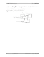
Page 54: ...nnections in the figure of board and module connection in and after 2 3 Power Supply Troubleshooting 1 Cable connection is described in the figure as line 2 Pin connection is described in the figure as arrow e g Connection of modem 2 2 CONFIDENTIAL TECRA M10 Maintenance Manual 960 685 ...

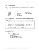
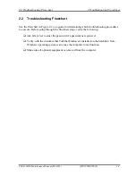
Page 55: ...r determining which troubleshooting procedures to execute Before going through the flowchart steps verify the following Ask him or her to enter the password if a password is registered Verify with the customer that Toshiba Windows is installed on the hard disk Non Windows operating systems can cause the computer to malfunction Make sure all optional equipment is removed from the computer ...

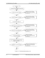
Page 56: ...2 Troubleshooting Procedures 2 2 Troubleshooting Flowchart Figure 2 1 Troubleshooting flowchart 1 2 2 4 CONFIDENTIAL TECRA M10 Maintenance Manual 960 685 ...

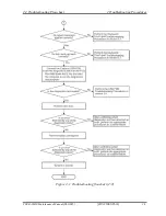
Page 57: ...2 2 Troubleshooting Flowchart 2 Troubleshooting Procedures Figure 2 1 Troubleshooting flowchart 2 2 TECRA M10 Maintenance Manual 960 685 CONFIDENTIAL 2 5 ...

Page 58: ...Keyboard Troubleshooting Procedures in Section 2 7 5 If an error is found on the touch pad test ONLY ONE TEST perform the touch pad Troubleshooting Procedures in Section 2 8 6 If an error is detected on the display test perform the Display Troubleshooting Procedures in Section 2 9 7 If an error is detected on the CD ROM DVD ROM test perform the Optical Disk Drive Troubleshooting Procedures in Sect...

Page 59: ...on the fingerprint sensor perform the Fingerprint Sensor Troubleshooting Procedures in Section 2 18 16 If a malfunction is detected on the Web camera perform the Web camera Troubleshooting Procedures in Section 2 19 17 If a malfunction is detected on the Intel Turbo Memory perform the Intel Turbo Memory Troubleshooting Procedures in Section 2 20 ...

Page 60: ...ower Status Check The following icons indicate the power supply status Battery icon DC IN icon The power supply controller displays the power supply status with the Battery icon and the DC IN icon as listed in the tables below Table 2 1 Battery icon Battery icon Power supply status Lights orange Battery is charged and the external DC is input It has no relation with ON OFF of the system power Ligh...

Page 61: ...tion the DC IN icon blinks orange It shows an error code When the icon is blinking perform the following procedure 1 Remove the battery pack and the AC adapter 2 Re attach the battery pack and the AC adapter If the icon is still blinking after the operation above check the followings Check 1 If the DC IN icon blinks orange go to Procedure 2 Check 2 If the DC IN icon does not light go to Procedure ...

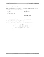
Page 62: ... orange The blink pattern indicates an error as shown below Start Off for 2 seconds Error code 8 bit 1 On for one second 0 On for half second Interval between data bits Off for half second The error code begins with the least significant digit Example Error code 11h Error codes are given in hexadecimal format Start 2 10 CONFIDENTIAL TECRA M10 Maintenance Manual 960 685 ...

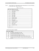
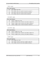
Page 63: ...ry 3 h 2nd battery 4 h S3V output 5 h E5V output 6 h E3V output 7 h 1R8 E1V output 8 h 1R5 P1V output 9 h PPV output A h 1R05M E1V output B h 1R8 E1V output C h PGV output D h 1R05 P1V output E h F h DC power supply AC adapter Error code Meaning 10h AC Adapter output voltage is over 16 5V 11h Common Dock output voltage is over 16 5V 12h Current from the DC power supply is over 4 95A 13h Current fr...

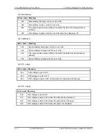
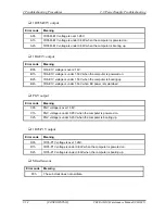
Page 64: ...h Second battery discharge current is over 0 5A 33h Second battery charge current is over 2 7A 34h The compensation value of 0A is not within the limits from design data 400mA 35h Second battery charge current is over 0 3A S3V output Error code Meaning 40h S3V voltage is over 3 47V 45h S3Vvoltage is under 3 14V 46h S3V voltage is under 3 14V or less when the computer is booting up E5V output Error...

Page 65: ...V voltage is over 2 16V 71h 1R8 E1V voltage is under 1 53V when the computer is powered on 72h 1R8 E1V voltage is under 1 53V when the computer is booting up 74h 1R8 E1V voltage is under 1 53V when BV power is maintained 1R5 P1V output Error code Meaning 80h 1R5 P1V voltage is over 1 80V 81h 1R5 P1V voltage is under 1 28V when the computer is powered on 82h 1R5 P1V voltage is under 1 28V when the ...

Page 66: ...53V when the computer is powered on B2h 1R8 E1V voltage is under 1 53V when the computer is booting up B4h 1R8 E1V voltage is under 1 53V when BV power is maintained PGV output Error code Meaning C0h PGV voltage is over 1 38V C1h PGV voltage is under 0 85V when the computer is powered on C2h PGV voltage is under 0 85V when the computer is booting up 1R05 P1V output Error code Meaning D0h 1R05 P1V ...

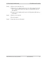
Page 67: ...12h Make sure the AC adapter and AC power cord are firmly plugged into the DC IN 15 V socket and wall outlet If the cables are connected firmly go to the following step Connect a new AC adapter and AC power cord If the problem still occurs go to Procedure 5 Check 3 In the case of error code 21h Go to Procedure 3 Check 4 For any other errors go to Procedure 5 ...

Page 68: ...does not light go to Procedure 4 Procedure 4 Charging Check Check if the power supply controller charges the battery pack properly Perform the following procedures Check 1 Make sure the AC adapter is firmly plugged into the DC IN jack Check 2 Make sure the battery pack is properly installed If it is properly installed go to Check 3 Check 3 The battery pack may be completely discharged Wait a few m...

Page 69: ...puter follow the steps described in Chapter 4 Replacement Procedures When AC adapter is connected Check 1 AC adapter may be faulty Replace the AC adapter with a new one If the problem still occurs perform Check 2 Check 2 System board may be faulty Replace the system board with a new one When AC adapter is not connected When driving with battery pack Check 1 Battery pack may be faulty Replace it wi...

Page 70: ...ng This section describes how to determine if the system board is malfunctioning or not Start with Procedure 1 and continue with the other procedures as instructed The procedures described in this section are Procedure 1 Message Check Procedure 2 Debugging Port Check Procedure 3 Diagnostic Test Program Execution Check Procedure 4 Replacement Check ...

Page 71: ...the F1 key as the message instructs the SETUP screen appears to set the system configuration If error message b appears often when the power is turned on replace the RTC battery If any other error message is displayed perform Check 2 a Bad HDD type Check system Then press F1 key b Bad RTC battery Check system Then press F1 key c Bad configuration Check system Then press F1 key d Bad memory size Ch...

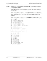
Page 72: ...r 21 is displayed go to the HDD Troubleshooting Procedures If error message 22 is displayed go to the USB FDD Troubleshooting Procedures 1 PIT ERROR 2 MEMORY REFRESH ERROR 3 TIMER CH 2 OUT ERROR 4 CMOS CHECKSUM ERROR 5 CMOS BAD BATTERY ERROR 6 FIRST 64KB MEMORY ERROR 7 FIRST 64KB MEMORY PARITY ERROR 8 VRAM ERROR 9 SYSTEM MEMORY ERROR 10 SYSTEM MEMORY PARITY ERROR 11 EXTENDED MEMORY ERROR 12 EXTEND...

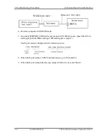
Page 73: ... of tool for debug port test 1 Serial Port model should make W3270 of Swich board is made to short circuit with a wire As for theposition of W3270 is refer to Appendix B 2 Connect the RS 232C cross cable to the connector CN3420 of the system board 3 Not a Serial Port model should connect a debug port test cable to connector CN3110 of a system board W3270 open 4 Connect the RS 232C Cross cable to t...

Page 74: ... CPU REAL mode Insert the FD for starting D port into FDD and input FD starting drive dport The D port status is displayed in the following form 6 When the D port status is FFFFh normal status go to Procedure 4 7 When the D port status falls into any status in Table 2 4 execute Check 1 2 22 CONFIDENTIAL TECRA M10 Maintenance Manual 960 685 ...

Page 75: ...00 EC KBC IC3001 BIOS ROM IC3400 Super I O BIOS ROM check F000 Problematic to BIOS ROM data BIOSROM IC3001 BIOS ROM F001 EC KBC rewriting check EC KBC KBC BIOSROM IC3200 EC KBC IC3000 BIOS ROM Initialization of EC Initialization of EC F002 Initialization of KBC F003 Initialization failure of EC F004 Initialization failure of EC HW failure EC KBC EC KBC BIOSROM IC3200 EC KBC IC3000 BIOS ROM F005 CP...

Page 76: ...CH IS1050 CPU Socket IC3000 BIOS ROM CPU setup CMOS setup F103 CMOS error CPU ICH CMOS BIOSROM IS1050 CPU Socket IC1600 ICH IC3000 BIOS ROM Resume branch BIOS processing reading F104 ROM read error ICH CMOS BIOSROM RAM CN1400 RAM Conn CN1410 RAM Conn IC1600 ICH IC3000 BIOS ROM F105 check of BIOS processing EC KBC EC TPM CPU IC3300 TPM IC3200 EC KBC IC3200 EEPROM IS1050 CPU Socket RAM setup F106 In...

Page 77: ...200 EC KBC CMOS initialization F10A setup of a setup item ICH CMOS EC KBC EC IC1600 ICH IC3200 EC KBC PnP device initialization F10B PCI device initialization PCI device IC2000 CARD Cont PCI ExpressCard setup F10C HDD setup ICH PCI registerMEM I O SATA controller EC KBC EC HDD IC1600 ICH HDD Cont CN1900 HDD Conn IC3200 EC KBC F10D Memory access check RAM CN1400 RAM Conn CN1410 RAM Conn F10E Memory...

Page 78: ... ICH DMAC ICH DMAC IC1600 ICH F11C Display setup VGA IC1200 VGA IC5000 VGA nVIDIA F11F Password processing EC KBC EC VGA ICH USB controller RAM IC1200 VGA IC5000 VGA nVIDIA CN1400 RAM Conn CN1410 RAM Conn IC1600 ICH setup of RAM data LAN initialization F120 LAN setup LAN Controller MCH PCI register VGA CPU BIOSROM IS1050 CPU Socket IC1200 MCH VGA IC5000 VGA nVIDIA IC3000 BIOS ROM IC4000 LAN Contro...

Page 79: ...r CPU RAM EC KBC KBC IS1050 CPU Socket IC1200 MCH CN1400 RAM Conn CN1410 RAM Conn IC3200 EC KBC AMT processing F148 AMT Mode only BIOS EXTENTION execution MCH ME BIOS ROM IC1200 MCH IC3000 BIOS ROM F149 AMT Mode only end of BIOS EXTENTION MCH ME BIOS ROM IC1200 MCH IC3000 BIOS ROM F14A AMT Mode only power supply OFF is set up from ME MCH ME ICH MEM I O BIOS ROM IC1200 MCH IC3000 BIOS ROM F14B AMT ...

Page 80: ... Preservation of PCI Preservation of PIT Display preservation Preservation of ICH PIC F13D Preservation of ICH DMAC ICH USB controller PIT controller PIC controller DMAC PCI register CPU HDD VGA PCI device IC1600 ICH PCI IS1050 CPU Socket CN1900 HDD Conn IC1200 VGA IC5000 VGA nVIDIA F13E Display setup Boot F141 HDD setup Boot VGA HDD ICH SATA controller IC1200 VGA IC5000 VGA nVIDIA F142 ROM Setup ...

Page 81: ...alization Initialization of a sound setup of ICH F12C setup of ICH PIC CPU ICH PITcontroller MEM I O CMOS I O PICcontroller SATA controller Soundcontroller Mod emcontroller PCI Expess USBcontroller PCI register Clock generator EC KBC EC KBC MCH RAM BIOSROM VGA IS1050 CPU Socket IC1600 ICH IC1000 CLKGEN IC3200 EC KBC IC1200 MCH VGA CN1400 RAM Conn CN1410 RAM Conn IC3000 BIOS ROM IC1200 VGA IC5000 V...

Page 82: ...nn CN1410 RAM Conn F133 setup of ICH DMAC ICH DMAC IC1600 ICH setup of ICH PCI CPU setup setup of ICH MEM IO Display setup setup of PIT F134 setup of ICH PIC ICH CMOS MEM I OS PIT controller PIC controller EC KBC EC KBC RAM BIOSROM CPU IC1600 ICH IC3200 EC KBC CN1400 RAM Conn CN1410 RAM Conn IC3000 BIOS ROM IS1050 CPU Socket F135 ICH Setup ICH IC1600 ICH F136 end of resume processing F137 RAM Setu...

Page 83: ...n the debug port test Check 1 If the D port is status F11Eh or F120h is displayed go to HDD Trouble shooting Procedure in Section 2 6 Check 2 If any other D port status error code is displayed perform Procedure 3 D port error code is as follows Error code Contents F003h or F004h SC initialization error F00Bh BIOS update error F117h Exception check error F121h Clock generator error ...

Page 84: ...s 1 System test 2 Memory test 3 Keyboard test 4 Display test 5 Floppy Disk test 6 Printer test It is not supported 7 Async test 8 Hard Disk test 9 Real Timer test 10 NDP test 11 Expansion test 12 CD ROM DVD ROM test 13 Only One test 14 Wireless LAN test 15 LAN Modem Bluetooth IEEE1394 test 16 Sound test If an error is detected during these tests go to Procedure 4 Procedure 4 Replacement Check Syst...

Page 85: ... Procedure 3 Connector Check and Replacement Check Procedure 1 FDD Head Cleaning Check FDD head cleaning is one option available in the Diagnostic Program After connecting USB FDD insert the Diagnostics Disk in the floppy disk drive Turn on the computer and run the test And then clean the FDD heads using the cleaning kit If the FDD still does not function properly after cleaning go to Procedure 2 ...

Page 86: ...Table 2 7 If any other errors occur while executing the FDD diagnostics test go to Check 1 Table 2 5 FDD error code and status Code Status 01h Bad command 02h Address mark not found 03h Write protected 04h Record not found 06h Media replaced 08h DMA overrun error 09h DMA boundary error 10h CRC error 20h FDC error 40h Seek error 60h FDD not drive 80h Time out error Not ready EEh Write buffer error ...

Page 87: ...connected to the following 4 ports System board x 1 ports and USB MDC board x 3 port Check 1 Make sure USB FDD is firmly connected to USB port If the connection is loose connect firmly and repeat Procedure 2 If the problem still occurs go to Check 2 NOTE When checking the connection be sure to check it with care for the followings 1 Cable can not be disconnected from the connector 2 Cable is conne...

Page 88: ... FDD to other USB port and check if it works properly If it does not work properly perform Check 3 Check 3 USB FDD may be faulty Replace it with a new one If the problem still occurs perform Check 4 Check 4 System board and USB MDC board may be faulty Replace it with a new one following the steps in Chapter 4 Replacement Procedures ...

Page 89: ... DOS system disk and start the computer Perform the following checks Check 1 Input C and press Enter If you cannot change to drive C go to Check 2 If you can change to drive C go to Procedure 2 Check 2 Input FDISK and press Enter Choose Display Partition Information from the FDISK menu If drive C is listed in the Display Partition Information go to Check 3 If drive C is not listed return to the FD...

Page 90: ...ROR After 5 seconds this message will disappear Check 2 If either of the following messages appears go to Check 3 If the following messages do not appear perform Check 4 Insert system disk in drive Press any key when ready or Non System disk or disk error Replace and press any key when ready Check 3 Using the SYS command of the DOS transfer the system to the 2 5 HDD If the system is not transferre...

Page 91: ... format by the test program refer to the Chapter 3 Check 1 Format the 2 5 HDD using DOS FORMAT command Type as FORMAT C S U If the 2 5 HDD can not be formatted perform Check 2 Check 2 Using the DOS FDISK command set the 2 5 HDD partition If the partition is not set go to Check 3 If it is set format the 2 5 HDD using MS DOS FORMAT command Check 3 Using the Diagnostic Disk format the 2 5 HDD with a ...

Page 92: ...es and statuses are described in Table 2 8 If an error code is not displayed but the problem still occurs go to Procedure 5 Table 2 6 2 5 Hard disk drive error code and status Code Status 05 HDD HDC NOT RESET ERROR 07 HDD DRIVE NOT INITIALIZE 09 HDD DMA BOUNDARY ERROR 0B HDD BAD TRACK ERROR BB HDD UNDEFINED ERROR 08 HDD OVERRUN ERROR DRQ ON 01 HDD BAD COMMAND ERROR 02 HDD ADDRESS MARK NOT FOUND 04...

Page 93: ...re loose reconnect firmly and repeat Procedure 1 If there is still an error go to Check 2 Check 2 The SATA HDD may be damaged Replace it with a new one following the instructions in Chapter 4 Replacement Procedures and check the operation If the problem still exists perform Check 3 Check 3 The HDD cable may be damaged Replace it with a new one following the instructions in Chapter 4 Replacement Pr...

Page 94: ...d Procedure 1 Diagnostic Test Program Execution Check Procedure 2 Connector Check and Replacement Check Procedure 1 Diagnostic Test Program Execution Check Execute the Keyboard Test DIAGNOSTIC TEST and Pressed key display test ONLY ONE TEST in the Diagnostic Program Refer to Chapter 3 Tests and Diagnostics for more information on how to perform the test program If an error occurs go to Procedure 2...

Page 95: ...ck 1 Make sure keyboard cable is firmly connected to system board If the connection is loose reconnect firmly and repeat Procedure 1 If the problem still occurs go to Check 2 Check 2 Keyboard may be faulty Replace it with a new one following the instructions in Chapter 4 Replacement Procedures If the problem still occurs perform Check 3 Check 3 System board may be faulty Replace it with a new one ...

Page 96: ...ures below as instructed Procedure 1 Diagnostic Test Program Execution Check Procedure 2 Connector Check and Replacement Check Procedure 1 Diagnostic Test Program Execution Check Execute the Touch pad test ONLY ONE TEST in the Diagnostic Program Refer to Chapter 3 Tests and Diagnostics for more information on how to perform the test program If an error occurs go to Procedure 2 If an error does not...

Page 97: ... loose reconnect firmly and repeat Procedure 1 If the problem still occurs go to Check 2 Check 2 Touch Pad or the cable may be faulty Replace it with a new one following the instructions in Chapter 4 Replacement Procedures If the problem still occurs perform Check 3 Check 3 Finger pad button board or the cable may be faulty Replace it with a new one following the instructions in Chapter 4 Replacem...

Page 98: ... to the computer s external monitor port then boot the computer The computer automatically detects the external monitor If the external monitor works correctly the internal LCD may be faulty Go to Procedure 3 If the external monitor appears to have the same problem as the internal monitor system board may be faulty Go to Procedure 2 Procedure 2 Diagnostic Test Program Execution Check The Display T...

Page 99: ... FL cable In addition fluorescent lamp is connected to FL inverter board by HV cable Their cables may be disconnected from system board or FL inverter board Disassemble the computer following the steps described in Chapter 4 Replacement Procedures If the connection is loose reconnect firmly and restart the computer If the problem still occurs go to Procedure 4 TECRA M10 Maintenance Manual 960 685 ...

Page 100: ...mp may be faulty Replace fluorescent lamp with a new one following the instructions in Chapter 4 Replacement Procedures and test the display again If the problem still occurs perform Check 2 Check 2 LCD FL cable may be faulty Replace FL LCD cable with a new one following the instructions in Chapter 4 Replacement Procedure and test the display again If the problem still occurs perform Check 3 Check...

Page 101: ...gnostics for more information on how to perform the test program Prepare the tools before the test If any error is detected by the test go to Procedure 2 Procedure 2 Connector Check and Replacement Check The SATA ODD may be disconnected or the SATA ODD ODD FPC or system board may be damaged Disassemble the computer following the steps described in Chapter 4 Replacement Procedures and perform the f...

Page 102: ...structions in Chapter 4 Replacement Procedures and check the operation If the problem still exists perform Check 3 Check 3 The ODD FPC may be damaged Replace it with a new one following the instructions in Chapter 4 Replacement Procedures If the problem still exists perform Check 4 Check 4 System board may be faulty Replace it with new one following the instructions in Chapter 4 Replacement Proced...

Page 103: ...m the test program If any error is detected perform Procedure 2 Procedure 2 Connector Check and Replacement Check MDC Modem Daughter Card is used as the modem for this computer MDC is connected to the system board If modem malfunctions the connection of cable board and module may be defective Otherwise they may be faulty Disassemble the computer following the steps described in Chapter 4 Replaceme...

Page 104: ...ay be faulty Replace it with a new one following the steps in Chapter 4 Replacement Procedure If the problem still occurs perform Check 4 Check 4 USB MDC board or the cable may be faulty Replace it with a new one following the instructions in Chapter 4 Replacement Procedures If the problem still occurs perform Check 5 Check 5 System board may be faulty Replace it with a new one following the instr...

Page 105: ... to perform the test program If any error is detected by the test go to Procedure 2 Procedure 2 Connector Check and Replacement Check LAN cable is connected to system board If LAN malfunctions the connection of the cable and board may be defective Otherwise they may be faulty Check 1 Make sure LAN cable is firmly connected to the LAN jack on the system board If the problem still occurs perform Che...

Page 106: ...k Procedure 3 Replacement Check Procedure 1 Transmitting Receiving Check Before starting the test make sure the wireless communication switch is set in the ON position Check 1 Execute Wireless LAN test program to check the transmitting receiving function of wireless LAN You will need a second computer that can communicate by wireless LAN Perform the test following the instructions described in Cha...

Page 107: ...n it On If the problem still occurs perform Check 2 Check 2 Make sure wireless LAN card PCI E Mini Card is firmly connected to the CN2600 on the system board If the connection is loose connect it firmly and perform Procedure 1 If the problem still occurs perform Check 3 Check 3 Make sure that wireless LAN antenna cables black and white are firmly connected to the connectors on Wireless LAN card If...

Page 108: ...r and then perform the following checks Check 1 Wireless LAN antenna may be faulty Replace it with a new one following the instructions in Chapter 4 Replacement Procedures If the problem still occurs perform Check 2 Check 2 Wireless LAN card may be faulty Replace it with a new one following the instructions in Chapter 4 Replacement Procedures If the problem still occurs perform Check 3 Check3 Syst...

Page 109: ...hat can communicate by the Bluetooth If the computer passes the test the function is correctly working If the computer does not pass the test go to check 2 Check 2 The Bluetooth module may be defective or damaged Replace it with a new one Then perform the test program again If the computer still does not pass the test go to Procedure 2 Procedure 2 Connector Check and Replacement Check The Bluetoot...

Page 110: ...ns in Chapter 4 Replacement Procedures and check the operation If the problem still exists perform Check 3 Check 3 The Bluetooth cable may be damaged Replace it with a new one following the instructions in Chapter 4 Replacement Procedures If the problem still exists perform Check 4 Check 4 The system board may be damaged Replace it with a new one following the instructions in Chapter 4 Replacement...

Page 111: ...Diagnostic Test Program Execution Check Execute the Sound test in Sound Test program disk Refer to Chapter 3 Tests and Diagnostics for more information on how to perform the test program If any error is detected by the test go to Procedure 2 Procedure 2 Connector Check The connection of sound system is shown in the following figure As the connection may be defective disassemble the computer and ch...

Page 112: ...the steps in Chapter 4 Replacement Procedures If the problem still occurs perform Check 4 Check 3 Internal microphone may be faulty Replace it with a new one following the steps in Chapter 4 Replacement Procedures If the problem still occurs perform Check 4 Check 4 Sound board may be faulty Replace it with a new one following the steps in Chapter 4 Replacement Procedures If the problem still occur...

Page 113: ...ia can be read If the card is not recognized or data are not red go to Procedure 2 Procedure 2 Connector Check and Replacement Check The Bridge media is connected to IS2140 on the system board Bridge media supports SD memory card SDIO card Memory stick Memory stick Pro xD Picture card Multimedia card Check 1 Bridge media and system board may be disconnected Make sure the Bridge media is firmly ins...

Page 114: ... following device is recognized on the Device Manager window Marvell Yukon 88E8053E PCI E Gigabit Ethernet Controller 2 2 is displayed in the PC with a built in LAN of Gigabit because the controller is the same one 2 is not displayed in the PC with a built in LAN of 10 100 Megabit 4 After confirmation take a Safety Remove procedure and pull out the Gigabit Ether ExpressCard 2 USB2 0 5in1 ExpressCa...

Page 115: ...as instructed When failed in Procedure 1 to Procedure 3 execute Procedure 4 Procedure 1 Setting Windows Log ON password Procedure 2 Registration of fingerprint Procedure 3 Authentication of fingerprint Procedure 4 Connector Check and Replacement Check CAUTION Scan your finger shown below 1 Lay your finger straight to the sensor and put lightly the first joint of your finger at the centerline of th...

Page 116: ...e previously enrolled fingerprints is selected again the latest information will be enrolled and any previous information over written 4 The Fingerprint Enrollment screen will be displayed and the tutorial will begin First click Replay video and confirm the proper movement for the finger you wish to register Then confirm the message displayed on this screen and ensure that there is a check mark in...

Page 117: ...Windows 2 In the Windows logon window put lightly the first joint of your finger registered and slide your finger sideways When authenticated Success is displayed in the fingerprint authentication display When not authenticated well warning message appears If you fail continually five times or more you can not use the fingerprint authentication about two minute When not authenticated type the pass...

Page 118: ... the cables are firmly connected to the Finger pad board and system board If the connection is loose reconnect firmly and repeat Procedure 1 If the problem still occurs go to Check 2 Check 2 Finger pad board or the cable may be faulty Replace it with a new one following the instructions in Chapter 4 Replacement Procedures If the problem still occurs perform Check 3 Check 3 System board may be faul...

Page 119: ...tware is installed the menu will stay on the screen but hide at the left edge of the screen Move the pointer to the left on the screen to show the menu When the menu appears double click the icon for Web Camera to operate the web camera If any troubles occur on recording replaying of still or moving images perform Procedure 2 Procedure 2 Connector Check and Replacement Check The connection of cabl...

Page 120: ...not be displayed web camera may be faulty Replace it with a new one following the steps in Chapter 4 Replacement Procedures If the problem still occurs perform Check 3 Check 3 System board may be faulty Replace it with a new one following the step in Chapter 4 Replacement Procedures 2 68 CONFIDENTIAL TECRA M10 Maintenance Manual 960 685 ...

Page 121: ...ment Check Procedure 1 Check on Windows OS Use the software Intel Turbo Memory Console which is originally prepared in the computer to check if the Intel Turbo Memory is operating without problems Start the Intel Turbo Memory Console and confirm the followings Check marks are attached to Enable Windows ReadyBoost and Enable Windows ReadyDrive The values for Windows ReadyBoost and Windows ReadyDriv...

Page 122: ...ollowing connection To disassemble the computer for the check follow the steps described in Chapter 4 If the connection is loose reconnect the card firmly If the problem still occurs perform Check 2 Check 2 The Intel Turbo Memory card may be faulty Replace it with a new one following the steps in Chapter 4 Replacement Procedures and check the operation again If the problem still occurs perform Che...

Page 123: ... CONFIDENTIAL Chapter 3 Tests and Diagnostics ...

Page 124: ...3 Tests and Diagnostics 3 ii CONFIDENTIAL TECRA M10 Maintenance Manual 960 685 3 ...

Page 125: ...nitial information setting tool 3 8 3 2 3 Heatrun test program 3 8 3 3 Setting of the hardware configuration 3 9 3 4 Heatrun Test 3 11 3 5 Subtest Names 3 12 3 6 System Test 3 14 3 7 Memory Test 3 16 3 8 Keyboard Test 3 17 3 9 Display Test 3 18 3 10 Floppy Disk Test 3 21 3 11 Printer Test 3 23 3 12 Async Test 3 25 3 13 Hard Disk Test 3 26 3 14 Real Timer Test 3 29 3 15 NDP Test 3 31 3 16 Expansion...

Page 126: ...lities 3 53 3 24 1 Function Description 3 53 3 24 2 Operations 3 54 3 25 System Configuration 3 58 3 25 1 Function Description 3 58 3 25 2 Operations 3 59 3 26 Wireless LAN Test Program Atheros 3 60 3 27 Wireless LAN Test Program Intel made a b g n Setting up of REF PC 3 62 3 28 Wireless LAN Test Program on DUT PC Intel made 3 67 3 29 LAN Modem Bluetooth IEEE1394 Test Program 3 71 3 29 1 LAN test ...

Page 127: ... Maintenance Manual 960 685 CONFIDENTIAL 3 v Tables Table 3 1 Subtest names 3 11 Table 3 2 Error codes and error status names 3 35 Table 3 3 Hard disk controller status register contents 3 38 Table 3 4 HDC Error register contents 3 39 ...

Page 128: ...3 Tests and Diagnostics 3 vi CONFIDENTIAL TECRA M10 Maintenance Manual 960 685 ...

Page 129: ...cluded in one of Diagnostic Disks The heatrun test is automatic test program that executes the some tests successively NOTE Before starting the diagnostics be sure to follow these steps 1 Check all cables are connected firmly 2 Exit any application and close Windows 3 Check if ALL Device is selected in the Device Config in SET UP menu After checking the diagnostics be sure to select Setup by OS in...

Page 130: ...lay supporting monitor ID Expansion test A CD test media TOSHIBA CD ROM TEST DISK or ABEX TEST CD ROM Sound test A DVD test media DVD ROM TEST DISK TSD 1 Sound test A music CD Sound test A CD RW test media CD ROM DVD ROM test A USB test module USB test A USB cable USB test LAN wraparound connector LAN test RGB wraparound connector Expansion test Module cable and RJ11 connector checker Modem test H...

Page 131: ... M10 Maintenance Manual 960 685 CONFIDENTIAL 3 3 The Diagnostics Disk Main T D 3 1 3 Heatrun test program The heatrun test starts automatically after the selection You will need the following equipment to perform this program The Diagnostics Disk Main T D ...

Page 132: ...tics menu T D press 3 and Enter To start the H W initial information setting tool press 1 and Enter To start the Heatrun test press 2 and Enter NOTE When replacing the system board be sure to execute the following procedures 1 Before replacing the system board execute subtest03 DMI information save in 3 4 Setting of the hardware configuration in order to save the DMI information from system board ...

Page 133: ...opyright TOSHIBA Corp 20XX DIAGNOSTICS MENU 1 DIAGNOSTIC TEST 2 ONLY ONE TEST 3 4 HEAD CLEANING 5 LOG UTILITIES 6 RUNNING TEST 7 FDD UTILITIES 8 SYSTEM CONFIGURATION 9 EXIT TO MS DOS NOTE To exit the DIAGNOSTIC TEST MENU press the Esc key If a test program is in progress press Ctrl Break to exit the test program If a test program is in progress press Ctrl C to stop the test program TECRA M10 Maint...

Page 134: ...ST 8 HARD DISK TEST 9 REAL TIMER TEST 10 NDP TEST 11 EXPANSION TEST 12 CD ROM DVD ROM TEST 88 ERROR RETRY COUNT SET FDD HDD 99 EXIT TO DIAGNOSTICS MENU NOTE Only when a 2nd HDD is installed in the computer There is a second hard disk message appears in the display Functions 1 through 12 are the Diagnostic Tests Function 88 sets the floppy disk drive and hard disk drive error retry count 0 255 To e...

Page 135: ...04 Quick charge 05 DMI read 99 Exit to DIAGNOSTIC TEST MENU NOTE The menu displayed by your computer may be slightly different from the one shown above Select the desired subtest number from the subtest menu and press Enter The following message will appear TEST LOOP YES or NO ERROR STOP YES or NO Use the right and left arrow keys to move the cursor to the desired option Selecting YES of TEST LOOP...

Page 136: ...est 3 Restarts the test from the error Selecting NO keeps the test running even if an error is found When an error occurred the error status is displayed and one error is added to the error counter Table 3 1 in section 3 6 describes the function of each test on the subtest menu Table 3 2 in section 3 19 describes the error codes and error status for each error 3 2 2 H W initial information setting...

Page 137: ...he item again Setting of the CPU set table Setting of the micro code Setting of the EHSS Inputting and writing of DMI information When the DMI information is displayed the following messages appear in order Input each information If you do not replace the PCB the DMI information should not be changed 1 Enter Model Name is displayed Input the computer s model name and press Enter e g DynaBook 2 Ent...

Page 138: ...contents and press Enter Subtest 02 DMI information save NOTE Before replacing the system board be sure to execute this subtest and save the DMI information to the floppy disk This is one of tools to copy the DMI information to a new PCB after replacing This subtest saves all the DMI data in a floppy disk Subtest 03 DMI information recovery This is one of tools to copy the DMI information to a new...

Page 139: ...d press Enter in the startup menu press Enter After selecting this test the same subtests as 3 23 RUNNING TEST is executed successively For more details on the procedure and test content refer to RUNNING TEST When the heatrun test ends following message appears in the display HEATRUN TEST END Press any key to continue Press any key and return to the startup menu ...

Page 140: ...Fan ON OFF Geyserville Quick charge DMI read 2 MEMORY 01 02 03 04 05 Conventional memory Protected Mode Protected Mode cache off Cache memory on off Stress 3 KEYBOARD 01 Pressed key code display 4 DISPLAY 01 02 03 04 05 06 07 VRAM read write for VGA Gradation for VGA Gradation for LCD Gradation Mode test for VGA All dot on off for LCD H pattern display LCD Brightness 5 FLOPPY DISK 01 02 03 04 05 S...

Page 141: ... to point receive Wraparound board 8 HARD DISK 01 02 03 04 05 06 07 08 09 Sequential read Address uniqueness Random address data Cross talk peak shift Partial Read Write specified address Read specified address Sequential write W R C specified address 9 REAL TIMER 01 02 03 Real time Backup memory Real time carry 10 NDP 01 NDP test 11 EXPANSION 01 02 PCMCIA wraparound Not supported RGB monitor ID 1...

Page 142: ...wing message will appear Fan number select 1 FAN 1 2 FAN 2 0 FAN 1 2 To check the CPU fan press 1 and Enter To check the VGA fan press 2 and Enter To check both CPU fan and VGA fan press 0 and Enter The following message will appear Fan test execute now CPU xxxxRpm GPU xxxxRpm Test Fan Revolution 0000RPM start Make sure the specified fan does not rotate and the message of fan revolution is 0000Rpm...

Page 143: ... test is ended This chip is not supported Subtest 04 Quick Charge This subtest checks the status for the quick charge Subtest 05 DMI read This subtest displays the information in the Flash ROM in the following format DMI Data Display Ver X XX Model Name XXXXXXXXXXX Version Number XXXXXXXXXXXX Serial Number XXXXXXXX UUID Number XXXXXXXXXXXXXXXXXXXXXXXXXXXXXXXX Model Number XXXXXX XXXXX PCN BND Numb...

Page 144: ...S file This subtest writes constant data and address data from 1MB to maximum MB and reads the new data and compares the result with the original data Subtest 03 Cache memory on off To test the cache memory a pass through write read comparison of 5Ah data is run repeatedly to the test area 7000 Program size to 7000 7FFF 32 KB to check the hit miss ratio on off status for CPU cache memory One test ...

Page 145: ...est 01 Pressed key code display When a key is pressed the scan code character code and key top name are displayed on the screen in the format shown below The Ins Lock Caps Lock Num Lock Scroll Lock Alt Ctrl Left Shift and Right Shift keys are displayed in reverse screen mode when pressed The scan codes character codes and key top names are shown in Appendix D KEYBOARD TEST IN PROGRESS 302000 Scan ...

Page 146: ...st 02 Gradation for VGA This subtest displays four colors red green blue and white from left to right across the screen from black to maximum brightness The display below appears on the screen when this subtest is executed To exit this subtest and return to the DISPLAY TEST menu press Enter Subtest 03 Gradation for LCD This subtest displays bands of gradations for mixed colors then for red green a...

Page 147: ...17 1024 768 64K Mode 118 1024 768 16M The display below appears on the screen when this subtest is executed Display example Mode 12 To exit this subtest and return to the DISPLAY TEST menu press Enter after displaying the Mode 118 Subtest 05 All dot on off for LCD This subtest displays an all white screen then an all black screen The display changes automatically every three seconds then returns t...

Page 148: ...HHHHHHHHHHHHHHHHHHHHHHHHHHHHHHHHHHHH HHHHHHHHHHHHHHHHHHHHHHHHHHHHHHHHHHHHHHHHHHHHHHHHHH HHHHHHHHHHHHHHHHHHHHHHHHHHHHHHHHHHHHHHHHHHHHHHHHHH HHHHHHHHHHHHHHHHHHHHHHHHHHHHHHHHHHHHHHHHHHHHHHHHHH HHHHHHHHHHHHHHHHHHHHHHHHHHHHHHHHHHHHHHHHHHHHHHHHHH HHHHHHHHHHHHHHHHHHHHHHHHHHHHHHHHHHHHHHHHHHHHHHHHHH HHHHHHHHHHHHHHHHHHHHHHHHHHHHHHHHHHHHHHHHHHHHHHHHHH To exit this subtest and return to the DISPLAY TEST menu ...

Page 149: ...e media mode and start track to be tested then press Enter Test start track Enter 0 dd 00 79 2 The Floppy Disk test contains five subtests that test the FDD The floppy disk test menu will appear after you select FDD test parameters FLOPPY DISK XXXXXXX XXX DIAGNOSTIC TEST VX XX Ctrl Break test end Ctrl C key stop SUB TEST XX PASS COUNT XXXXX ERROR COUNT XXXXX WRITE DATA XX READ DATA XX ADDRESS XXXX...

Page 150: ... 04 only Track No Head No Subtest 01 Sequential read This subtest performs a Cyclic Redundancy Check CRC that continuously reads all the tracks track 0 to 39 0 to 79 on a floppy disk Subtest 02 Sequential read write This subtest continuously writes data pattern B5ADADh to all the tracks track 0 to 39 0 to 79 on a floppy disk The data is then read and compared to the original data Subtest 03 Random...

Page 151: ...following message will appear after selecting the subtest 01 to 03 of the printer test channel 1 XXXXh channel 2 XXXXh channel 3 XXXXh Select the channel number 1 3 The printer I O port address is specified by the XXXXh number The computer supports three printer channels Select the printer channel number and press Enter to execute the selected subtest Subtest 01 Ripple Pattern This subtest prints ...

Page 152: ...nt This subtest prints the various print types shown below Subtest 03 Wraparound NOTE To execute this subtest a printer wraparound connector must be connected to the computer s printer port This subtest checks the output and bi directional modes of the data control and status lines through the parallel port wraparound connector 34M741986G01 Both output and bi directional modes are tested 3 24 CONF...

Page 153: ...oint to point send NOTE To execute subtests 01 and 02 each computer must have access to the other computer s infrared port This subtest sends 20h through 7Eh data to the receive side then receives the sent data and compares it to the original data through the FIR SIR port Subtest 02 FIR SIR Point to point receive This subtest is used with subtest 01 described above This subtest receives the data f...

Page 154: ...only once If it exists use it to back up the pre installed software then use the Backup utility in the System Tools folder to back up the entire disk including the user s files Refer to the operating system instructions When a 2nd HDD is installed the following messages will appear after selecting the hard disk test from the DIAGNOSTIC TEST MENU Test drive number select 1 HDD 1 2 HDD 2 0 HDD 1 2 1...

Page 155: ...t digit of the STATUS number indicates the drive being tested and the last two digits indicate the error status code as explained in table 3 2 of the section 3 19 Subtest 01 Sequential read This subtest is a sequential reading of all the tracks on the HDD starting at track 0 When all the tracks on the HDD have been read the test starts at the maximum track and reads the tracks on the HDD sequentia...

Page 156: ...r 2DB6DB 6 cylinder D25114 7 cylinder Subtest 05 Partial Read This subtest reads 1GB data that is in minimum middle and maximum address of the HDD area Subtest 06 Write specified address This subtest writes specified data to a specified cylinder and head on the HDD Subtest 07 Read specified address This subtest reads data which has been written to a specified cylinder and head on the HDD Subtest 0...

Page 157: ...ew date PRESS ENTER KEY TO EXIT TEST 2 If the current date is not correct input the correct date at the Enter new date prompt and press Enter 3 The following messages will appear Current date XX XX XXXX Current time XX XX XX Enter new time PRESS ENTER KEY TO EXIT TEST 4 If the current time is not correct input the correct time in 24 hour format To enter press Shift The time is updated To exit the ...

Page 158: ... date and time are erased This subtest checks the real time clock increments making sure the date and time are displayed in the following format Current date 12 31 1999 Current time 23 59 58 The real time increments are automatically executed and the following is displayed Current date 01 01 2000 Current time 00 00 00 PRESS Enter KEY TO EXIT TEST To exit the test press Enter ...

Page 159: ...ICS TEST MENU press Enter and follow the directions on the screen CAUTION Judge the existence of high speed operation processor by 1bit of the composition byte If exists the bit is 1 Test only when the high speed operation processor exists Subtest 01 NDP test This test checks the following functions of NDP Control word Status word Bus Addition Multiplication ...

Page 160: ...wraparound connector is required This subtest checks the following signal line of the PC card slot Address line REG CE 1 CE 2 line Data line Speaker line Wait line BSY BVD1 line This subtest is executed in the following order Sub Address Good Bad Contents 01 00001 00001 nn nn xx xx Address line REG CE 1 CE 2 nn A0 90 80 00 02 00002 ww rr Data line ww write data rr read data 03 00003 Speaker line 0...

Page 161: ...E To execute this subtest monitor supporting EDID Extended Display Identification Data is required Connect a wraparound connector to CRT monitor for the test of ID acquisition This subtest is executed by using VESA command CAUTION It becomes NG because the priority is given to the internal monitor in a simultaneous display mode ...

Page 162: ...r ABEX TEST CD ROM TCDR 702 and DVD ROM TEST DISK TSD 1 For the subtest 04 use a CD RW on the market Subtest 01 Sequential read This subtest is a sequential reading of one block units 2K bytes of all the logical addresses Subtest 02 Read specified address This subtest reads one block data from a specified address Subtest 03 Random address data This subtest reads one block data and multi block data...

Page 163: ... ADAPT ROM SENSING ERROR 1st Batt ROM SENSING ERROR 2nd Batt ROM THORMISTOR ERROR 1 ROM THORMISTOR ERROR 2 ROM THORMISTOR ERROR 3 Memory 01 02 DD RAM PARITY ERROR RAM PROTECTED MODE NO CHANGE RAM CACHE MEMORY ERROR Keyboard FE FD F0 F1 F2 F3 F4 F5 F6 F7 F8 F9 FA EF ED USB GET DESCR ERROR FIRST USB SET ADDRESS ERROR HUB GET DESCR ERROR Top 8B HUB GET DESCR ERROR Whole HUB SET CONFIGURATION ERROR HU...

Page 164: ... PRT TIME OUT PRT FAULT PRT SELECT LINE PRT OUT OF PAPER PRT POWER OFF PRT BUSY LINE ASYNC 01 02 04 08 10 20 40 80 88 05 06 RS232C DTR ON TIME OUT RS232C CTS ON TIME OUT RS232C RX READY TIME OUT RS232C TX FULL TIME OUT RS232C PARITY ERROR RS232C FRAMING ERROR RS232C OVERRUN ERROR RS232C LINE STATUS ERROR RS232C MODEM STATUS ERROR SIR TIME OUT ERROR FIR TIME OUT ERROR HDD 05 07 09 0B BB 08 01 02 04...

Page 165: ...ROCESSOR NDP CONTROL WORD ERROR NDP STATUS WORD ERROR NDP BUS ERROR NDP ADDITION ERROR NDP MULTIPLAY ERROR EXPANSION C1 C3 C4 C5 C6 C7 C8 CB CC CE CF ADDRESS LINE ERROR CE 1 LINE ERROR CE 2 LINE ERROR DATA LINE ERROR WAIT LINE ERROR BSY LINE ERROR BVD1 LINE ERROR ZV Port ERROR NO PCMCIA CARD TYPE ERROR ZV_CONT ERROR CD ROM DVD ROM 01 02 03 04 05 06 09 11 20 40 80 90 B0 BAD COMMAND ILLEGAL LENGTH U...

Page 166: ...displays the HDC error register The contents of the HDC status register and error register are listed in Tables 3 3 and 3 4 Table 3 3 Hard disk controller status register contents Bit Name Description 7 BSY Busy 0 HDC is ready 1 HDC is busy 6 DRY Drive ready 0 Hard disk drive is not ready to accept any command 1 Hard disk drive is ready 5 DWF Drive write fault 0 DWF error is not detected 1 Write f...

Page 167: ...detected 6 UNC Uncorrectable 0 There is no uncorrectable data error 1 Uncorrectable data error has been detected 5 Not used 4 IDN Identification 0 Not used 1 There is no ID field in the requested sector 3 Not used 2 ABT Abort 0 Not used 1 Illegal command error or command abort 1 TK0 Track 0 0 The hard disk found track 0 during a recalibrate command 1 The hard disk could not find track 0 during a r...

Page 168: ... the DIAGNOSTIC MENU and press Enter The following menu appears in the display ONLY ONE TEST Menu QOSMIO G20 1 Pressed Key Display 2 Touch pad 3 Wireless communication Switch 4 USB Port select menu 5 LED 6 Button 7 Acceleration sensor 8 Docker Dock Undoc 9 Fan control 99 Exit to Common Test Press test number 1 9 Select the subtest number you want to test and press Enter To return to the DIAGNOSTIC...

Page 169: ... display as shown below When any key is pressed the corresponding key on the screen changes to the key character that was pressed Holding a key down enables the auto repeat function that causes the key s display character to blink Press Del Enter to end the test IF TEST OK Press Dell Enter key TECRA M10 Maintenance Manual 960 685 CONFIDENTIAL 3 41 ...

Page 170: ...itch When moving your finger on the touch pad towards the upper left the POINTING display changes according to the following illustration If a touch pad switch is pressed the BUTTONS displays appear on the right side one by one The parameters appear above the BUTTONS 1 or 2 corresponding to the pressed touch pad switch highlights To end this subtest press two touch pad switches at the same time 3 ...

Page 171: ...N position Then following message appears in the display Wireless communication Switch OFF After Sliding the switch to OFF position return to the ONLY ONE TEST menu automatically Subtest 04 USB NOTE When executing this subtest USB test module and USB cable must be connected This subtest checks if USB port works properly The following menu appears in the display USB Port Select XXXXXXXXX 0 Port 0 F...

Page 172: ...s in the display to execute the test HDD Access LED test Confirm the LED of HDD status blinks properly Press any key and following message appears in the display Caps Num Overlay BT W LAN LED test Confirm each LED lights properly 1 Press Caps Lock key Caps on off 2 Press Fn F10 key Arrow on off 3 Press Fn F11 key Num on off 4 Slide BT W LAN switch L R on off Press Enter and following message appea...

Page 173: ... ends without an error Press any key return to each Steps if NG or Press any key message apprears Press the Toshiba Presentation button after the following message appears Step2 X 1 2 Press Function button Presentation button OK message appears in the display if the test ends without an error Press any key return to each Steps if NG or Press any key message apprears If the test ends successfully t...

Page 174: ...at desk with vertical plane to get the stability of machine 2 The vertical wall or plane is necessary 3 Prevent the machine from shake or shock Vertical plane Flat desk Set the machine against the vertical plane with the Front upward Example The figure below shows the name and position of each side 3 46 CONFIDENTIAL TECRA M10 Maintenance Manual 960 685 Right side Left side Back Front Top heaven su...

Page 175: ...ane on the flat desk with the right side of machine upward Then press Enter to detect the data on this setting of machine The following message appears in the display The front establishes in the upper direction Press Enter key Set the machine against the vertical plane on the flat desk with the front of machine upward Then press Enter to detect the data on this setting of machine The following me...

Page 176: ...nu When the display returns to the ONLY ONE TEST menu remove the Express Port Replicator from the computer Subtest 09 Fan control This subtest checks if FAN works properly The following message appears in the display in order Start low speed rotation Waits 8 seconds Start reading of rotation Waits 3 seconds Start Hight speed rotation Waits 8 seconds Start reading of rotation Waits 3 seconds FAN Lo...

Page 177: ...orm this program 3 21 2 Operations 1 Selecting test 4 from the DIAGNOSTIC MENU and pressing Enter displays the following messages DIAGNOSTICS FLOPPY DISK HEAD CLEANING VX XX Mount cleaning disk s on drive s Press any key when ready 2 Remove the Diagnostics Disk from the FDD then insert the cleaning disk and press Enter 3 When the cleaning start message appears the FDD head cleaning has begun 4 The...

Page 178: ...USB FDD when you perform the DIAGNOSTIC PROGRAM from the DVD ROM The data is stored in floppy disk The error information is displayed in the following order 1 Error count CNT 2 Test name Subtest number TS No 3 Pass count PASS 4 Error status STS 5 FDD HDD or memory address ADDR 6 Write data WD 7 Read data RD 8 HDC status HSTS 9 Error status name ERROR STATUS NAME If the power switch is turned off t...

Page 179: ...ENTIAL 3 51 1 Next 2 Prev 3 Exit 4 Clear 5 Print 6 FD Log Read 7 FD Log Write 2 The error information displayed on the screen can be manipulated by the following number keys The 1 key scrolls the display to the next page The 2 key scrolls the display to the previous page The 3 key returns to the Diagnostic Menu The 4 key erases all error log information in RAM The 5 key outputs the error log infor...

Page 180: ... detects the number of floppy disk drives connected to the computer for the FDD test 3 23 2 Operations 1 Select 6 from the Diagnostic Menu and press Enter the following messages will appear in the display in order FDD write read test Y N Printer wrap around test Y N Serial wrap around test Y N CD ROM DVD ROM test Y N 2 To execute the test press Y yes and Enter To cancel the test press N no and Ent...

Page 181: ...rom the Toshiba MS DOS FORMAT command This program can format a floppy disk in the following formats a 2DD Double sided double density double track 96 135 TPI MFM mode 512 bytes 9 sectors track b 2HD Double sided high density double track 96 135 TPI MFM mode 512 bytes 18 sectors track 2 COPY This program copies data from a source floppy disk to a target floppy disk 3 DUMP This program displays the...

Page 182: ...ng message Type select 0 2DD 3 2HD c Select a media drive type number and press Enter A message similar to the one below will be displayed Warning Disk data will be destroyed Insert work disk into drive A Press any key when ready d Remove the Diagnostics Disk from the FDD insert the work disk and press any key The following message will be displayed when the FDD format is executed FDD TYPE TRACK X...

Page 183: ...as started FDD TYPE TRACK XXX FDD TYPE HEAD X FDD TYPE SECTOR XX Copy start track head XXX X d The following message will appear Insert target disk into drive A Press any key when ready e Remove the source disk from the FDD then insert a formatted work disk and press any key The following message will appear and start copying to the target disk track head XXX X f When the amount of data is too lar...

Page 184: ...g message will appear Select a media mode 2HD media mode 1 1 20MB 2 1 44MB 3 1 23MB e The following message will appear Insert source disk into drive A Press any key when ready f Insert a source disk and press any key and the following message will appear Max address Track XXXX Head XX Sector XX Track number g Set the track number head number and sector number you want to dump The system will acce...

Page 185: ...y 1 up 2 down 3 end l The following message will appear Selecting 2 returns to the FDD UTILITIES MENU Another dump 1 Yes 2 No 5 HDD ID READ program Selecting HDD ID displays the following HDD ID configuration HDD ID Read VX XX Drive 1 Drive 2 Model No XXXXXXX XXXXXXX NOTE Only when a 2nd HDD is installed Drive 2 message appears in the display Press Enter to return to the FDD UTILITIES MENU ...

Page 186: ...version 1st ID 2nd ID 4 Boot ROM version 5 EC KBC version 6 PS Microprocessor version 7 SVP parameter version Panel Manufacture code Product code 8 Micro code revision Processor number 9 Total Memory Size Conventional memory 10 Battery code 11 HWSC 12 FSB Voltage 13 Printer Adapter 14 ASYNC Adapter 15 Math co processors 16 Floppy Disk Drive Track Head Sector 17 Hard Disk Drive Sector Drive size Ma...

Page 187: ... XX PS Micon Version VX XX SVP Par Version VX XX Panel XXXXXXXXX Manu XXXX Prod XXXX Micro code Revision VX XX Processor XXXh Total Memory Size XXXXXXMB Conventional Memory XXXKB Battery Code XXXXXXXXXXXX HWSC XXXXXXX FSB XXXXXMHz Voltage XEh X Printer Adapter LPT1 XXXX LPT2 XXXX LPT3 XXXX X ASYNC Adapter COM1 XXXX COM2 XXXX COM3 XXXX X Math CO Processor X Floppy Disk Drive s Track XX Head XX Sect...

Page 188: ...dows programs Check of the wireless LAN card type 1 Slide the wireless communication switch to ON position 2 Check the card type according to the following procedure Click Start All Programs TOSHIBA Utilities PC Diagnostic Tool Check the Network If the Atheros AR5007EG 11b g Atheros AR5006EX 11a b g Atheros AR9281 11b g n or Atheros 9280 11a b g n is shown the correct card is installed in the comp...

Page 189: ... the computer finds any AP Access Point the antenna marks like as follows will appear It shows the antenna cables are surely connected to the wireless LAN card 3 The following message will appear if the antenna cables are not connected to the wireless LAN card or no available access point is found In this case check the antenna cable connection to the wireless LAN card by disassembling the compute...

Page 190: ... 11a 11aAP AP for check of 11b 11bAP AP for check of 11g 11gAP Make the security functions of AP WEP WPA etc invalid REF Reference PC Cross cable DUT Device Under Testing DUT Device Under Testing REF Reference PC 11a b g AP Cross cable Configuration of equipment for transmitting receiving test How to setup the REF PC Set up the wireless LAN environment needed for the test before the start of Respo...

Page 191: ...agnostics Open My Computer window and click My Network places on the left column Click View network connections on the left column TECRA M10 Maintenance Manual 960 685 CONFIDENTIAL 3 63 The Network Connections window appears Double click Local Area Connection Network Connections window ...

Page 192: ... Connection Properties window Local Area Connection Properties window Select Protocol on the Select Network Component Type window and click Add button 3 64 CONFIDENTIAL TECRA M10 Maintenance Manual 960 685 Select Network Component Type window Click Have Disk button on the Select Network Protocol window Select Network Protocol window ...

Page 193: ...k window The Select Network Protocol window appears again In the Network Protocol DDK PACKET Protocol will appear Then click OK to start the installation Select Network Protocol window When the installation is completed Local Area Connection Properties will appear Confirm that the DDK PACKET Protocol is added Click Close button to finish the setup of REF PC Local Area Connection Properties window ...

Page 194: ...om DUT via AP OS available Windows XP only How to start Double click WTWINSVR icon How to start 1 Double click wtwinsvr icon The following screen will appear Startup screen of wtwinsvr program 2 Enter the number of Network Adapter used on REF PC enter 1 for example above Then the following screen will appear Start the test program on DUT Screen while running the wtwinsvr program The REF PC is wait...

Page 195: ...tics disk for wireless LAN test into the Floppy Disk Drive Turn on the power while pressing U The following menu appears in the display Intel WiFi Link 5100 5300 Maintenance T D Menu 1 Communication test of 11a mode for 5100 5150 module 2 Communication test of 11b mode for 5100 5150 module 3 Communication test of 11g mode for 5100 5150 module 4 All the tests of WiFi Link 5100 5150 Module MAC Check...

Page 196: ... the test NG message will appear in the display When pressing any key the following message is displayed 11a Communication Test NG tx a antenna rx a antenna Press any key and return to the test menu Subtest02 Communication test of 11b mode for 5100 5150 module Two antenna type This subtest execute transmitting receiving test in 802 11b mode using the main antenna If a defective is not found during...

Page 197: ...eturn to the test menu Subtest04 All the tests of WiFi Link 5100 5150 Module MAC Check communication test Two antenna type All the tests is executed in the order of Communication test of 11a mode Communication test of 11b mode and Communication test of 11g mode When any error has detected the test finishes Subtest05 Communication test of 11a mode for 5100 5150 module Three antenna type This subtes...

Page 198: ...eturn to the test menu Subtest07 Communication test of 11g mode for 5100 5150 module Three antenna type This subtest execute transmitting receiving test in 802 11g mode using the main antenna If a defective is not found during the test OK message will appear in the display Press any key and return to the test menu If a defective is found during the test NG message will appear in the display When p...

Page 199: ...on the power The following message will appear Microsoft Windows XX Startup Menu 1 LAN 2 Modem 3 Bluetooth 4 IEEE1394 Enter a choice Press the number you want to test and press Enter NOTE It is impossible to go back to startup menu once you choose the test Therefore LAN Modem Bluetooth IEEE1394 test can not be executed successively 3 29 1 LAN test To execute LAN test press 1 and Enter The followin...

Page 200: ...it receive test COMPLETED Repeat count 00000 Error count 00000 LOOPBACK TEST 100Mbps Auto negotiation TxRx Test Destination Address xxxxxxxxxxxx Source Address xxxxxxxxxxxx 100Base TX Full Duplex TRANSMIT RECEIVE NOTE The menu displayed by your computer may be slightly different from the one shown above If a defective is found NG message will appear in the display 3 72 CONFIDENTIAL TECRA M10 Maint...

Page 201: ...er The following message will appear Testing adaptor hit ESC to abort External Loopback Test PASSED Testing completed Loopback Test Complete 1000Base Auto negotiation TxRx Test CE Test Complete NOTE The menu displayed by your computer may be slightly different from the one shown above If a defective is found NG message will appear in the display TECRA M10 Maintenance Manual 960 685 CONFIDENTIAL 3 ...

Page 202: ...odem test press 2 and Enter Following message will appear Modem loopback test ICHx MDC Test Program with Modem Sound Line Test Version X X Scorpio Modem Initialize OK Digital Loopback Test OK RJ11 Connector Check LED Operator s Check OK is displayed when a error is detected NG is display when a error is not detected NOTE The menu displayed by your computer may be slightly different from the one sh...

Page 203: ...h the Bluetooth function is also available A Bluetooth card should be installed on the target computer Install the Bluetooth function by clicking All Programs TOSHIBA Bluetooth Bluetooth Settings Test procedure 1 Enable the Bluetooth function of the responder device 2 Make sure the wireless communication switch of the target computer is set to ON position 3 Right click the Bluetooth icon on the lo...

Page 204: ...ce 7 When the BT Bluetooth address of the responder device appears the Bluetooth card and antenna connection are OK If the BT address of the responder device does not appear check the Bluetooth card condition and antenna cable connection to the Bluetooth card by disassembling the computer following the steps described in Chapter 4 Replacement Procedures 3 76 CONFIDENTIAL TECRA M10 Maintenance Manu...

Page 205: ...ress test number 1 3 To execute the TEST select the test number you want to execute and press Enter Subtest01 Transmit Receive test NOTE Before executing subtest 01 be sure to execute subtest 02 in the responder machine This program checks the data transporting between responder machine and target machine and compare them with the original data through the IEEE1394 cable Subtest02 Responder set Th...

Page 206: ...the sound on Windows OS 1 Play a music file 2 click TOSHIBA utility PC diagnostic tool to test the sound Please check operation of speakers by one of methods 3 30 3G Test program Therefore please test the sound on Windows OS All the programs included in EU870 test CD are install A procedure should look at ToshibaTestTools_ReleaseNotes txt Please uninstall after the completion of a EU870 test ...

Page 207: ...sor Password 3 HDD Password a HDD b HDD Password Mode c User Password d Master Password 5 Boot Priority a Boot Priority b HDD Priority 6 Others a Core Multi Processing b Dynamic CPU Frequency Mode c Execute Disable Bit Capability d Virtualization Technology e Trusted Execution Technology f Auto Power On g Beep Volume h Diagnostic Mode i USB Sleep and Charge 7 Configuration 8 Battery a Battery Save...

Page 208: ...D b ODD c SATA Controller Mode 11 PCI Bus 12 Display a LCD Display Stretch 13 Peripheral a Internal Pointing Device 14 Legacy Emulation a USB KB Mouse Legacy Emulation b USB FDD Legacy Emulation c USB Memory BIOS Support Type 15 PCI LAN a Built in LAN 16 Security Controller a TPM b Hide TPM 17 Intel R AMT a MEBx SETUP ...

Page 209: ...31 SETUP 3 Tests and Diagnostics 3 31 2 Accessing the SETUP Program While pressing ESC turn on the power Then press F1 The following display appears TECRA M10 Maintenance Manual 960 685 CONFIDENTIAL 3 81 ...

Page 210: ...3 Tests and Diagnostics 3 31 SETUP 3 82 CONFIDENTIAL TECRA M10 Maintenance Manual 960 685 ...

Page 211: ...ed item requires the system to reboot the following message is displayed Are you sure Y N The changes you made will cause the system to reboot 2 To make other changes press N Repeat the steps above 3 To accept the changes press Y NOTE You can press Esc to quit at any time without saving changes SETUP asks you to confirm that you do not want to save your changes When SETUP is displayed at the next ...

Page 212: ...sword This option allows you to set or reset the user password for power on Registered A password has been registered Not Registered Change or remove the password Default a Supervisor Password This setting which is displayed on the first page of the setup screen allows you to register a Supervisor Password of the computer Registered Supervisor Password has been registered Not Registered Supervisor...

Page 213: ...set in the HDD password Mode For details refer to the User s Manual 5 Boot Priority a Boot Priority Use this option to set the priority for booting of the computer and the priority for the HDD for booting HDD FDD CD ROM LAN The computer looks for bootable files in the following order HDD FDD CD ROM and LAN Default FDD HDD CD ROM LAN The computer looks for bootable files in the following order FDD ...

Page 214: ...configuration for the Core Multi Processing is carried out in the BIOS setup program Enabled is Dual Core mode Disabled is Single Core mode Enabled Enables Core Multi Processing functions Default Disabled Disables Core Multi Processing functions b Dynamic CPU Frequency mode Core2 model only Use this option to choose a setting from the followings Dynamically Switchable Enables Intel CoreTM Duo proc...

Page 215: ...ization Technology installed in the CPU Intel Virtualization Technology is the technique that allows one machine to operate as multiple virtual machines Enabled Enables Virtualization Technology Disabled Disables Virtualization Technology Default e Trusted Execution Technology Core2 model only Permission prohibition of Trusted Execution Technology are set up Trusted Execution Technology is the sec...

Page 216: ...n Built in LAN is set to Enabled To activate this function use the AC adapter On Battery The following settings can be changed when the Wake up on LAN is Enabled Enabled Wake up on LAN function whenoperating from the battery Disabled Wake up on LAN function whenoperating from the battery Default NOTE 1 Do not remove the AC adaptor and battery pack at the same time when you use this feature If you ...

Page 217: ...en switched to Hibernation Mode Default Disabled No action is taken even if the remaining battery power is about to run out while the system is in Sleep Mode g Beep Volume This Option sets up the volume of a Beep sound Medium High OFF Low h Diagnostic Mode This option enables disables the HW Diagnostic test function Enabled Disables the HW Diagnostic test function Default Disabled Enables the HW D...

Page 218: ...r the test end select Setup by OS 7 Battery a Battery Save Mode This option is used to select Full Power Low Power or User Setting of the battery save mode When you select the battery save mode the followings will appear Full Power The following shows full power settings Low Power The following shows low power settings NOTE Display of the LCD Brightness will be changed in the condition below 1 Ope...

Page 219: ...ty Bright Full brightness for high visibility Semi Bright Less than full brightness for saving power Cooling Method Maximum Performance If the CPU becomes too hot the fan turns on automatically in a high speed to cool down the CPU Performance If the CPU becomes too hot the fan turns on automatically When the CPU temperature falls to a normal range the fan turns off Battery optimized If the CPU bec...

Page 220: ...tion of Enhanced C States on the following conditions Enabled This lowers the power consumption Default Disabled This does not lower the power consumption 8 I O ports This option controls settings for the parallel port NOTE Do not assign the same interrupt request level and I O address to the serial port and PC card a Serial Use this option to set the COM level for the serial port The serial port ...

Page 221: ...the Serial ATA Port Number It is for information only and cannot be changed Serial ATA Port4 d SATA Controller Mode This feature sets the SATA Controller Mode AHCI Sets AHCI which is the mode for VistaTM default Compatibility Sets the mode for legacy OS Use this mode when the driver corresponding to AHCI is not used 10 PCI Bus This option displays the interrupt level for the Card Bus in the comput...

Page 222: ...h pad Enabled Enables the touch pad Default Disabled Disables the touch pad 13 LEGACY EMULATION a USB KB Mouse Legacy Emulation This option sets the Legacy support condition of the USB keyboard and the USB mouse Enabled Enables LEGACY support Default USB keyboard USB mouse are available without the driver Disabled Disables LEGACY support b USB FDD Legacy Emulation This option sets the Legacy suppo...

Page 223: ...ontroller c TPM Disables the security controller called TPM Trusted Platform Module When the cursor is on the Enable Disable and the Space is pressed message is displayed and the PC waits Y or N key input by the user When Y is pressed it is sets to Enable Disable After changing the cursor could not be moved on the TPM tem This option can be changed after rebooting Disabled Disables the TPM Default...

Page 224: ...3 Tests and Diagnostics 3 31 SETUP 3 96 CONFIDENTIAL TECRA M10 Maintenance Manual 960 685 ...

Page 225: ...Chapter 4 Replacement Procedures CONFIDENTIAL ...

Page 226: ...4 Replacement Procedures 4 ii CONFIDENTIAL TECRA M10 Maintenance Manual 960 685 ...

Page 227: ...4 6 Fin cover 4 21 4 7 HDD 4 22 4 8 Optical disk drive DVD ROM DVD Super Multi drive 4 25 4 9 Keyboard 4 27 4 10 SW board 4 32 4 11 SIM board 4 35 4 12 Wireless LAN card 4 37 4 13 3G card 4 39 4 14 Robson card 4 41 4 15 Speaker 4 43 4 16 Cover assembly and Base assembly 4 46 4 17 MDC modem USB board 4 50 4 18 RGB harness RJ45 harness 4 53 4 19 Serial board 4 56 4 20 System board 4 58 4 21 GFX boar...

Page 228: ...4 86 4 31 Camera module Wireless LAN antenna 3G antenna 4 92 4 32 LCD harness 4 101 4 33 LCD mask 4 104 4 34 Hinge 4 107 4 35 Fluorescent Lamp 4 110 4 35 1 Replacing the 14 1 inch WXGA LG Fluorescent Lamp 4 111 4 35 2 Replacing the 14 1 inch WXGA Samsung Fluorescent Lamp 4 119 4 35 3 Replacing the 14 1 inch WXGA LG Fluorescent Lamp 4 122 4 35 4 Replacing the 14 1 inch WXGA CSV LG Fluorescent Lamp ...

Page 229: ...optical disk drive 4 26 Figure 4 14 Removing the KB holder 1 4 27 Figure 4 15 Removing the KB holder 2 4 28 Figure 4 16 Removing the keyboard 1 4 29 Figure 4 17 Removing the keyboard 2 4 30 Figure 4 18 Removing the SW board 4 32 Figure 4 19 Removing the insulator COVER UP INSULATOR 4 33 Figure 4 20 Removing the SW board FFC 4 34 Figure 4 21 Removing the SIM board 4 35 Figure 4 22 Removing the wire...

Page 230: ...ing the PC card unit 4 70 Figure 4 46 Removing the RTC battery 4 72 Figure 4 47 Removing the sound board microphone harness 4 74 Figure 4 48 Removing the battery lock 4 76 Figure 4 49 Removing the touch pad fingerprint sensor board 1 4 78 Figure 4 50 Removing the touch pad fingerprint sensor board 2 4 79 Figure 4 51 Removing the touch pad fingerprint sensor board 3 4 80 Figure 4 52 Removing the to...

Page 231: ... Removing the hinge 1 4 107 Figure 4 67 Removing the hinge 2 4 108 Figure 4 68 to 4 75 Replacing 14 1 inch LG fluorescent lamp WXGA 1 to 8 4 111 to 4 118 Figure 4 76 to 4 79 Replacing 14 1 inch Samsung fluorescent lamp WXGA 1 to 4 4 119 to 4 121 Figure 4 80 to 4 87 Replacing 14 1 inch LG fluorescent lamp WXGA 1 to 8 4 122 to 4 129 Figure 4 88 to 4 95 Replacing 14 1 inch LG fluorescent lamp WXGA CS...

Page 232: ...4 Replacement Procedures 4 viii CONFIDENTIAL TECRA M10 Maintenance Manual 960 685 ...

Page 233: ...he numbers in the chart indicate the relevant section numbers in this manual In all cases when removing an FRU the battery pack must also be removed When repairing an FRU that is the potential cause of a computer fault use the chart to determine the order in which FRUs need to be removed Chart Notation The chart shows the case for the following example Removing the MDC modem USB board All FRUs dow...

Page 234: ...e following items ITEM Parts List ITEM No PART NAME Quantity 50 COVER ASSY 1 COVER ASSY 64 64 A TOUCH PAD 1 ITEM Parts List ITEM No PART NAME Quantity 51 LCD COVER ASSY 1 75 CAMERA MODULE 1 LCD COVER ASSY 46 47 2 4 5 2GHZ ANTENNA 1 Parts which can not be reused are 1 Touch pad 2 Camera module 3 Wireless LAN antenna 2 4 5 2GHZ ANTENNA and 4 3G antenna ...

Page 235: ... card WL LAN 802 11a g n 15 RTC battery BTN N H BATTERY 19 DVD ROM DRIVE 19 A Optical disk drive DVD SUPER MULTI DRIVE 45 HDD harness S ATA HARNESS 46 2 4 5 2GHZ ANTENNA 47 Wireless LAN antenna 2 4 5 2GHZ ANTENNA 50B Brake hinge L BH L ASSY 50C Brake hinge R BH R ASSY 65 TOUCH PAD 67 Unit dual pad TPAD PLT FP ASSY S01 M2 0 3C S THIN HEAD T SCREW M2X3CR S02 M2 0 2 7 Unique FHG SCREW M2X2 7 S03 M3 0...

Page 236: ...e computer is disconnected from an AC power source Remove any metal jewelry or accessories such as necklaces bracelets or rings in order to reduce the risk of electric shock Never work with wet or damp hands 3 Be careful of edges and corners as these may cut CAUTION 1 When you change a component be sure the replacement component meets the required specifications Never use foreign parts to avoid an...

Page 237: ...iagnostic tests described in Chapter 2 to determine which FRU is the cause of the fault 5 Do not perform any unnecessary work Always work in accordance with the disassembly and re assembly procedures in this manual 6 Keep parts removed from the computer in a safe place away from the computer where they will not be damaged or interfere with your work 7 Disassembling requires the removal of a large ...

Page 238: ...orrect position Pull the cable to ensure that it is securely connected For spring connectors lift up the stopper frees the cable and allow it to be pulled out To reconnect hold the stopper in the up position and insert the cable then lower the stopper to secure the cable Pull the cable to ensure that it is securely connected For back flip connectors lift up the flip plate frees the cable and allow...

Page 239: ...ect screw may damage the thread or screw head and result in the FRU not being securely fastened in place After installing FRUs check that the computer operates correctly Tools and Equipment For your safety and the safety of the people around you it is important that you use Electrostatic Discharge ESD equipment Correctly utilizing of the equipment increases the percentage of successful repairs and...

Page 240: ...ba recommends that you use an electric screw driver for quick and easy operations M2 2mm 0 167 N m 1 7 kgf cm M2 5 2 5mm 0 294 N m 3 0 kgf cm M3 3mm 0 549 N m 5 6 kgf cm NOTE To prevent damage to THIN HEAD screws use type 0 bit philips screwdriver Press along the axis of the screwdriver while turning the screw This is because the contact area between the screw and driver is less than for a pan hea...

Page 241: ...own Odd numbered length screws White Grip area Special length screw Blue Special grip Even numbered length screws Yellow Odd numbered length screws Pink Special length screw Green Special length screw means screws whose length is indicated in an integral number to the first decimal places such as 2 5 mm 2 6 mm and so on TECRA M10 Maintenance Manual 960 685 CONFIDENTIAL 4 9 ...

Page 242: ...s including the types and lengths of the screws are indicated on the computer body Format Screw type Screw length mm Screw shape B Bind screw F Flat head screw S Super thin head screw T Tapping screw U Other screws Unique screws pan head stud etc Example B6 6mm BIND screw Screw color material B Black Nickel C Silver Non Hexavalent Chromate U Other screws Unique screws such as stud etc ...

Page 243: ...ry pack 1 Turn off the power of the computer 2 Disconnect the AC adapter and other external devices from the computer 3 Turn the computer face down 4 Release the battery lock and remove the battery pack while sliding the battery release latch as shown in the figure below Battery pack Battery release latch Battery lock Figure 4 1 Removing the battery pack NOTE Dispose of the used battery pack in ac...

Page 244: ...perated handled or disposed correctly Dispose always the used battery pack in accordance with the laws and ordinances of your local authority Use only the batteries approved by Toshiba NOTE Check the battery s terminals visually If they are dirty wipe them clean with a dry cloth 1 Turn off the power of the computer 2 Disconnect the AC adapter and all other external devices to the computer 3 Insert...

Page 245: ...w and refer to Figure 4 2 and 4 3 1 Slide the SIM card release latch in the direction as shown in the figure below 2 Turn up the SIM card holder in the direction as shown in the figure below SIM card release latch SIM card holder Figure 4 2 Removing the SIM card 1 TECRA M10 Maintenance Manual 960 685 CONFIDENTIAL 4 13 ...

Page 246: ...alling the SIM card To install the SIM card follow the steps below and refer to Figure 4 2 and 4 3 1 Set the SIM card into the SIM card holder 2 Lay the SIM card holder down and lock the SIM card release latch while sliding it in the opposite direction as shown in the figure 4 2 4 14 CONFIDENTIAL TECRA M10 Maintenance Manual 960 685 ...

Page 247: ...the manuals of the computer system you are using 1 Press the eject button for the PC card to extend the button 2 Press the extended eject button to pop the PC card out 3 Grasp the PC card and pull it out Eject button PC card Figure 4 4 Removing the PC card Installing the PC card To install the PC card follow the steps below and refer to Figure 4 4 1 Insert the PC card into the card slot 2 Push it ...

Page 248: ...ns in each Bridge Media manual or the manuals of the computer system you are using 1 Push the Bridge media It will pop out partly when you release so pull out the card For an instance SD card is described in the figure 4 5 Bridge media SD card Figure 4 5 Removing the Bridge media Installing the Bridge media To install the Bridge media follow the steps below and refer to Figure 4 5 1 Insert the Bri...

Page 249: ...h any instructions in the Smart card manual or the manuals of the computer system you are using 1 Pull out the Smart card from the card slot Smart card Figure 4 6 Removing the Smart card Installing the Smart card To install the Smart card follow the steps below and refer to Figure 4 6 1 Insert the Smart card into the card slot 2 Push it carefully to ensure a firm connection TECRA M10 Maintenance M...

Page 250: ...owered off Removing a memory module with the power on might damage the module or the computer itself Do not touch the connectors on the memory module or on the computer Dust and stains on the connectors may cause memory access problems Never press hard or bend the memory module 1 Turn over the computer 2 Loosen the screw fixing the memory cover 3 Remove the memory cover Memory cover Screw Figure 4...

Page 251: ...e 4 Replacement Procedures 4 Open the left and right latches outside and remove the memory module s Memory module Latch Latch Figure 4 8 Removing the memory module TECRA M10 Maintenance Manual 960 685 CONFIDENTIAL 4 19 ...

Page 252: ...er on might damage the module or the computer itself Never press hard or bend a memory module 1 Insert the memory module s into the connector s slantwise and press it to connect firmly CAUTION After installing the memory module make sure that the memory module is secured with the left and right latches 2 Install the memory cover and secure it with the screw 3 When the power of the computer is turn...

Page 253: ... Fin cover To remove the Fin cover follow the steps below and refer to Figure 4 9 1 Push down the hook and remove the fin cover while sliding it in the direction in the figure below Hook Fin cover Figure 4 9 Removing the fin cover Installing the Fin cover To install the Fin cover follow the steps below and refer to Figure 4 9 1 Set the fin cover into the slot and slide it to engage the hook TECRA ...

Page 254: ... loss or damage to the device 1 Remove the following screw securing the HDD cover M2 5 5B FLAT HEAD screw 1 2 Insert your finger into the slot and lift the HDD cover to remove 3 Remove the HDD assembly from the slot and disconnect it from the connector on the HDD harness HDD cover M2 5 5B FLAT HEAD Slot HDD assembly HDD harness Figure 4 10 Removing the HDD assembly 4 22 CONFIDENTIAL TECRA M10 Main...

Page 255: ...ollowing screws and separate the HDD and HDD holder M3 0 4C FLAT HEAD screw 4 M3 0 4C FLAT HEAD HDD HDD Holder M3 0 4C FLAT HEAD M3 0 4C FLAT HEAD M3 0 4C FLAT HEAD Figure 4 11 Removing the HDD TECRA M10 Maintenance Manual 960 685 CONFIDENTIAL 4 23 ...

Page 256: ... to Figure 4 10 and 4 11 1 Set the HDD to the HDD Holder and secure them with the following screws M3 0 4C FLAT HEAD screw 4 2 Set the connector of the HDD harness upward and connect the HDD assembly to the connector of the HDD harness Lay the HDD assembly down into the slot 3 Set the HDD cover and secure it with the following screw M2 5 5B FLAT HEAD screw 1 ...

Page 257: ...ected because of some failure open the disc tray by inserting a slender object about 15 mm such as a straightened paper clip into the eject hole near the eject button 1 Remove the following screws securing the optical disk drive M2 5 5B FLAT HEAD screw 2 2 Remove the optical disk drive assembly from the slot while pushing it in the direction as shown in the figure below Optical disk drive assembly...

Page 258: ...sk drive To install the Optical disk drive follow the steps below and refer to Figure 4 12 to 4 13 1 Set the ODD rear bracket to the optical disk drive and secure them with the following screws M2 0 2 7C Unique screw 2 2 Set the ODD side bracket to the optical disk drive and secure them with the following screw M2 0 3C S THIN HEAD screw 1 3 Insert the optical disk drive assembly into the slot to c...

Page 259: ...CAUTION As the keytop may fall out when handling the keyboard always hold it by the frame and do not touch the keytop 1 Turn over the computer 2 Insert your fingers into the slits and release both sides of latches of the KB holder at the rear KB holder Slit Slit Figure 4 14 Removing the KB holder 1 TECRA M10 Maintenance Manual 960 685 CONFIDENTIAL 4 27 ...

Page 260: ... 9 Keyboard 3 Open the display and make it flat 4 Insert your finger into the slot on left side and remove the KB holder KB holder Slot Figure 4 15 Removing the KB holder 2 4 28 CONFIDENTIAL TECRA M10 Maintenance Manual 960 685 ...

Page 261: ...M2 5 4B FLAT HEAD screw 2 6 Lift the top edge of the keyboard while releasing the latches and turn the keyboard face down on the palm rest M2 5 4B FLAT HEAD M2 5 4B FLAT HEAD Latch Keyboard Latch Latch Figure 4 16 Removing the keyboard 1 TECRA M10 Maintenance Manual 960 685 CONFIDENTIAL 4 29 ...

Page 262: ...he figure below to remove M2 5 10B FLAT HEAD screw 1 8 Disconnect the keyboard flexible cable from the connector CN3230 on the system board and remove the keyboard M2 5 10B FLAT HEAD KB support plate Keyboard Keyboard flexible cable CN3230 Figure 4 17 Removing the keyboard 2 4 30 CONFIDENTIAL TECRA M10 Maintenance Manual 960 685 ...

Page 263: ... plate with the following screw M2 5 10B FLAT HEAD screw 1 CAUTION Do not put the keyboard flexible cable on the KB support plate Fold down the keyboard flexible cable as shown in the figure below Keyboard flexible cable 4 Turn the keyboard face up and set it in place Extra portion of the keyboard cable must be put under the KB support plate 5 Secure the keyboard with the following screws M2 5 4B ...

Page 264: ...refer to Figure 4 18 to 4 20 1 Disconnect the SW board FFC from the connector CN9600 on the SW board 2 Push down the hook and slide the SW board in the direction as shown in the figure below to remove it CN9600 SW board FFC SW board Hook Figure 4 18 Removing the SW board 4 32 CONFIDENTIAL TECRA M10 Maintenance Manual 960 685 ...

Page 265: ...oard 4 Replacement Procedures 3 Peel off the insulator COVER UP INSULATOR Insulator COVER UP INSULATOR Figure 4 19 Removing the insulator COVER UP INSULATOR TECRA M10 Maintenance Manual 960 685 CONFIDENTIAL 4 33 ...

Page 266: ... to Figure 4 18 to 4 20 1 Connect the SW board FFC to the connector CN9600 on the SW board CAUTION Make sure that the SW board FFC is connected securely to the connector on the SW board The connector of the SW board is not a lock type 2 Slide the SW board into the slot to set it 3 Connect the SW board FFC to the connector CN9500 on the system board 4 Stick the insulator COVER UP INSULATOR in place...

Page 267: ...onnector CN9570 on the system board 2 Remove the SIM board from the slot while peeling the double sided tapes 3 Disconnect the SIM board FFC from the connector CN9670 on the back of the SIM board CN9570 SIM board FFC SIM board CN9670 Hole Hole Guide Double sided tape Double sided tape Double sided tape Figure 4 21 Removing the SIM board TECRA M10 Maintenance Manual 960 685 CONFIDENTIAL 4 35 ...

Page 268: ...steps below and refer to Figure 4 21 1 Connect the SIM board FFC to the connector CN9670 on the back of the SIM board 2 Set the SIM board to the slot with the holes into the guides NOTE When installing a new SIM board peel off three separators of the double sided tapes on the SIM board 3 Connect the SIM board FFC to the connector CN9570 on the system board ...

Page 269: ...ess LAN card white cable from Main and black cable from Aux using an antenna coaxial cable disconnector 2 Remove the following screws securing the wireless LAN card M2 0 4B BIND screw 2 3 Disconnect the wireless LAN card from the connector on the system board M2 0x4B BIND Wireless LAN card Wireless LAN antenna cable Wireless LAN antenna cable Figure 4 22 Removing the wireless LAN card TECRA M10 Ma...

Page 270: ...ollow the steps below and refer to Figure 4 22 1 Insert the wireless LAN card to the connector on the system board slantwise and press it to connect firmly 2 Push down the wireless LAN card and secure it with the following screws M2 0 4B BIND 2 3 Connect the wireless LAN antenna cables to the connectors white cable to Main and black cable to Aux on the wireless LAN card ...

Page 271: ...tenna cables from the 3G card using an antenna coaxial cable disconnector 2 Remove the following screws securing the 3G card M2 0 4B BIND screw 2 3 Disconnect the 3G card from the connector on the system board M2 0x4B BIND 3G card 3G antenna cable red 3G antenna cable blue Slit Figure 4 23 Removing the 3G card TECRA M10 Maintenance Manual 960 685 CONFIDENTIAL 4 39 ...

Page 272: ... follow the steps below and refer to Figure 4 23 1 Insert the 3G card to the connector on the system board slantwise and press it to connect firmly 2 Push down the 3G card and secure it with the following screws M2 0 4B BIND 2 3 Connect the 3G antenna cables to the connectors on the 3G card and arrange the antenna cables through the slit ...

Page 273: ...d follow the steps below and refer to Figure 4 24 1 Remove the following screws securing the Robson card M2 0 4B BIND screw 2 2 Disconnect the Robson card from the connector on the system board M2 0x4B BIND Robson card Figure 4 24 Removing the Robson card TECRA M10 Maintenance Manual 960 685 CONFIDENTIAL 4 41 ...

Page 274: ...0 685 Installing the Robson card To install the Robson card follow the steps below and refer to Figure 4 24 1 Insert the Robson card to the connector on the system board slantwise and press it to connect firmly 2 Push down the Robson card and secure it with the following screws M2 0 4B BIND 2 ...

Page 275: ...r To remove the speaker follow the steps below and refer to Figure 4 25 to 4 27 1 Disconnect the speaker harness from the connector CN6150 on the system board CN6150 Speaker harness Figure 4 25 Removing the speaker 1 TECRA M10 Maintenance Manual 960 685 CONFIDENTIAL 4 43 ...

Page 276: ...edures 4 15 Speaker 2 Peel off the two insulators SQUARE INSULATOR and turn up the insulators Insulator SQUARE INSULATOR Insulator Figure 4 26 Removing the insulator 4 44 CONFIDENTIAL TECRA M10 Maintenance Manual 960 685 ...

Page 277: ...re 4 27 Removing the speaker 2 Installing the Speaker To install the speaker follow the steps below and refer to Figure 4 25 to 4 27 1 Install the speakers left and right to the speaker slots 2 Turn up the insulators and arrange the speaker cables into the slot 3 Connect the speaker harness to the connector CN6150 on the system board 4 Stick the two insulators SQUARE INSULATOR in place TECRA M10 M...

Page 278: ...w the steps below and refer to Figure 4 28 to 4 30 1 Close the display and turn over the computer 2 Remove the following screws M2 5 16B FLAT HEAD screw 3 16 in the figure below M2 5 10B FLAT HEAD screw 8 10 in the figure below M2 5 5B FLAT HEAD screw 2 5 in the figure below 5 16 16 5 16 10 10 10 10 10 10 10 10 Figure 4 28 Removing the cover assembly and base assembly 1 4 46 CONFIDENTIAL TECRA M10...

Page 279: ...FFC 6 Disconnect the Smart card FFC from the connector CN2170 on the system board and remove the core from the Smart card FFC 7 Remove the following screws M2 5 10B FLAT HEAD screw 4 M2 5x10B FLAT HEAD Touch pad FFC Connected to CN9550 Smart card FFC Connected to CN2170 LCD harness Connected to CN5000 Bluetooth harness Connected to CN4440 Camera harness Connected to CN9540 Acetate tape Core Figure...

Page 280: ...mbly and Base assembly 8 Separate the cover assembly and base assembly while releasing the latches Cover assembly Base assembly Figure 4 30 Removing the cover assembly and base assembly 3 4 48 CONFIDENTIAL TECRA M10 Maintenance Manual 960 685 ...

Page 281: ...on the system board Stick the acetate tape in place NOTE Set the core next to the connector portion of the Smart card FFC and stick the acetate tape on them Acetate tape Core Connector 3 Connect the touch pad FFC Bluetooth harness camera harness and LCD harness to the connector CN9550 CN4440 CN9540 and CN5000 on the system board 4 Turn over the computer and secure the cover assembly and base assem...

Page 282: ...move the following screws securing the MDC modem M2 0 4B BIND screw 2 2 Take out the RJ11 harness from the slot and lift the MDC modem straight above to remove it from the connector CN3010 on the USB board 3 Disconnect the RJ11 harness from the connector on the MDC modem MDC modem RJ11 harness M2 0x4B BIND CN3010 Figure 4 31 Removing the MDC modem 4 50 CONFIDENTIAL TECRA M10 Maintenance Manual 960...

Page 283: ... system board and connector CN9660 on the USB board 5 Remove the USB board from the slot of the base assembly while pushing the latches in the direction as shown in the figure below USB board USB harness CN9560 CN9660 Latch Figure 4 32 Removing the USB board TECRA M10 Maintenance Manual 960 685 CONFIDENTIAL 4 51 ...

Page 284: ... 2 Connect the USB harness to the connector CN9560 on the system board and connector CN9660 on the USB board 3 Connect the RJ11 harness to the connector on the MDC modem 4 Connect the MDC modem to the connector CN3010 on the USB board by pressing it carefully and secure it with the following screws M2 0 4B BIND screw 2 CAUTION Remove and connect the MDC modem from on the USB board perpendicularly ...

Page 285: ...nd refer to Figure 4 33 and 4 34 1 Turn up the insulator and disconnect the RGB harness from the connector CN9510 on the system board 2 Remove the following screw and take out the RGB harness from the slot of the base assembly M2 5 6C Tapping screw 1 RGB harness CN9510 M2 5x6C Tapping Insulator Figure 4 33 Removing the RGB harness TECRA M10 Maintenance Manual 960 685 CONFIDENTIAL 4 53 ...

Page 286: ...Disconnect the RJ45 harness from the connector CN4100 on the system board and remove the RJ45 harness from the slot of the base assembly RJ45 harness CN4100 Insulator Figure 4 34 Removing the RJ45 harness 4 54 CONFIDENTIAL TECRA M10 Maintenance Manual 960 685 ...

Page 287: ...ure 4 33 and 4 34 1 Turn up the insulator and connect the RJ45 harness to the connector CN4100 on the system board 2 Set the RJ45 harness into the slot of the base assembly and arrange it to the guides 3 Connect the RGB harness to the connector CN9510 on the system board 4 Set the RGB harness into the slot of the base assembly and arrange it to the guides 5 Secure the RGB harness with the followin...

Page 288: ...ial board FFC from the connector CN9520 on the system board 2 Push the hook to release and remove the serial board from the slot of the base assembly 3 Disconnect the serial board FFC from the connector CN9620 on the back of the serial board Serial board FFC CN9520 CN9620 Serial board Hook Figure 4 35 Removing the serial board 4 56 CONFIDENTIAL TECRA M10 Maintenance Manual 960 685 ...

Page 289: ... To install the serial board follow the steps below and refer to Figure 4 35 1 Connect the serial board FFC to the connector CN9620 on the back of the serial board 2 Set the serial board into the slot of the base assembly while engaging it to the hook 3 Connect the serial board FFC to the connector CN9520 on the system board ...

Page 290: ... 2 After replacing the system board execute the subtest03 DMI ggginformation recovery and subtest01 Entry of the DMI information gggin order to copy the DMI information and system configuration ggginformation 3 Also update the BIOS and EC KBC with the latest ones according to the steps described in Appendix G and Appendix H Removing the System board To remove the system board follow the steps belo...

Page 291: ...d 4 Replacement Procedures M2 5 6C Tapping screw 1 System board Glass tape M2 5x6C Tapping DC IN jack CN9530 Sound board FFC Figure 4 36 Removing the system board TECRA M10 Maintenance Manual 960 685 CONFIDENTIAL 4 59 ...

Page 292: ...nect the DC IN harness and HDD harness from the connector CN8800 and CN1900 on the back of the system board CN8800 CN1900 HDD harness DC IN harness Figure 4 37 Removing the DC IN harness HDD harness 4 60 CONFIDENTIAL TECRA M10 Maintenance Manual 960 685 ...

Page 293: ...d refer to Figure 4 36 to 4 37 1 Connect the DC IN harness and HDD harness to the connector CN8800 and CN1900 on the back of the system board 2 Set the system board in place and secure it with the following screw s M2 5 6C Tapping screw 1 3 Set the DC IN jack into the slot 4 Connect the sound board FFC to the connector CN9530 on the system board and stick the glass tape in place ...

Page 294: ...ollow the steps below and refer to Figure 4 38 and 4 39 1 Remove the following screws and disconnect the GFX board with the GFX fin from the connector CN5900 on the system board M2 0 4B BIND screw 2 CN5900 GFX board GFX fin M2 0x4B BIND Figure 4 38 Removing the GFX board GFX fin 1 4 62 CONFIDENTIAL TECRA M10 Maintenance Manual 960 685 ...

Page 295: ... the following screws and separate the GFX fin and GFX board M2 0 3C S THIN HEAD screw 4 GFX board GFX fin M2 0x3C S THIN HEAD M2 0x3C S THIN HEAD Cool sheet Figure 4 39 Removing the GFX board GFX fin 2 TECRA M10 Maintenance Manual 960 685 CONFIDENTIAL 4 63 ...

Page 296: ... new cool sheet on the GFX board in place NOTE Do not reuse the cool sheet Be sure to use a new cool sheet 2 Set the GFX fin to the GFX board and secure them with the following screws M2 0 3C S THIN HEAD screw 4 NOTE When securing the GFX fin be sure to secure the screws in the order of the number marked 1 to 4 on the fin 3 Connect the GFX board with the GFX fin to the connector CN5900 on the syst...

Page 297: ... heat sink plate M2 0 4B BIND screw 4 3 Remove the following screws and CPU fin with the DC fan M2 0 4B BIND screw 2 NOTE When removing the heat sink plate and CPU fin be sure to remove the screws in the reverse order of the number marked 4 to 1 and 2 to 1 on the heat sink plate and board spring of the CPU fin Figure 4 40 Removing the CPU fin DC fan 1 Fan harness Heat sink plate M2 0x4B BIND CPU f...

Page 298: ...n DC fan 4 Remove the following screws and separate the DC fan and CPU fin M2 5 4B FLAT HEAD screw 2 CPU fin DC fan M2 5x4B FLAT HEAD Cool sheet Figure 4 41 Removing the CPU fin DC fan 2 4 66 CONFIDENTIAL TECRA M10 Maintenance Manual 960 685 ...

Page 299: ...e cam counterclockwise on the CPU socket by 180 degrees with a flat blade screwdriver 6 Remove the CPU Figure 4 42 Removing the CPU CAUTION When removing the CPU lift it up right above Otherwise pins of the CPU may be damaged TECRA M10 Maintenance Manual 960 685 CONFIDENTIAL 4 67 ...

Page 300: ...cam of the CPU socket is in the unlock OPEN position 2 Set the CPU to the correct position in the CPU socket Make sure the position of the CPU triangle mark is correct to avoid damaging pins on the CPU 3 Lock the CPU by rotating clockwise the cam on the CPU socket by 180 degrees with a flat blade driver Mark Figure 4 43 Installing the CPU 4 68 CONFIDENTIAL TECRA M10 Maintenance Manual 960 685 ...

Page 301: ...et Be sure to use a new cool sheet 15X15XT1 0 7 Set the DC fan to the CPU fin and secure them with the following screws M2 5 4B FLAT HEAD screw 2 8 Set the CPU fin with the DC fan in place and secure it with the following screws M2 0 4B BIND screw 2 NOTE When securing the CPU fin be sure to secure the screws in the order of the number marked 1 to 2 on the board spring of the fin 9 Set the heat sin...

Page 302: ...to Figure 4 45 1 Remove the following screws securing the PC card unit M2 0 3C Tapping screw 2 M2 0 8C Tapping screw 2 2 Remove the PC card unit while releasing the latches M2 0x3C Tapping Latch PC card unit M2 0x3C Tapping M2 0x8C Tapping M2 0x8C Tapping Figure 4 45 Removing the PC card unit 4 70 CONFIDENTIAL TECRA M10 Maintenance Manual 960 685 ...

Page 303: ...al 960 685 CONFIDENTIAL 4 71 Installing the PC card unit To install the PC card unit follow the steps below and refer to Figure 4 45 1 Set the PC card unit while engaging the latches and secure it with the following screws M2 0 3C Tapping screw 2 M2 0 8C Tapping screw 2 ...

Page 304: ...battery follow the steps below and refer to Figure 4 46 1 Peel off the glass tape and disconnect the RTC battery harness from the connector CN9300 on the sound board 2 Remove the insulator RTC BATT INSULATOR from the slot 3 Open the insulator RTC BATT INSULATOR and take out the RTC battery Insulator RTC BATT INSULATOR RTC battery CN9300 RTC battery harness Glass tape Figure 4 46 Removing the RTC b...

Page 305: ...he RTC battery To install the RTC battery follow the steps below and refer to Figure 4 46 1 Set the RTC battery into the insulator RTC BATT INSULATOR 2 Set the insulator RTC BATT INSULATOR to the slot 3 Connect the RTC battery harness to the connector CN9300 on the sound board and stick the glass tape in place ...

Page 306: ...he following screws and sound board microphone harness from the slot M2 5 4B FLAT HEAD screw 2 3 Disconnect the microphone harness from the connector CN6050 on the sound board 4 Disconnect the sound board FFC from the connector CN9630 on the sound board M2 5x4B FLAT HEAD 4 74 CONFIDENTIAL TECRA M10 Maintenance Manual 960 685 Figure 4 47 Removing the sound board microphone harness Sound board CN963...

Page 307: ...sound board microphone harness follow the steps below and refer to Figure 4 47 1 Connect the sound board FFC to the connector CN9630 on the sound board 2 Connect the microphone harness to the connector CN6050 on the sound board 3 Set the sound board microphone harness to the slot and secure it with the following screws M2 5 4B FLAT HEAD screw 2 4 Stick the glass tape in place ...

Page 308: ...L INSULATOR and remove the battery lock L from the slot 3 Remove the battery lock button R while pushing latches inside to release them 4 Remove the battery lock R from the slot CAUTION When removing the battery locks be careful not to lose the springs Spring 4 76 CONFIDENTIAL TECRA M10 Maintenance Manual 960 685 Figure 4 48 Removing the battery lock Battery lock button L Battery lock button R Bat...

Page 309: ... Figure 4 48 1 Insert the sticks of the battery lock L and battery lock R into the springs 2 Turn up the insulator BATT LOCK L INSULATOR and set the battery lock L to the slot 3 Set push the battery lock button L to the battery lock L until the latches are engaged 4 Set the battery lock R to the slot 5 Set push the battery lock button R to the battery lock R until the latches are engaged ...

Page 310: ...ow the steps below and refer to Figure 4 49 to 4 52 1 Turn up the insulator TPAD PLT INSULATOR and remove the following screws M2 5 4B FLAT HEAD screw 4 2 Peel off the insulator SQUARE INSULATOR M2 5x4B FLAT HEAD Insulator TPAD PLT INSULATOR M2 5x4B FLAT HEAD Insulator TPAD PLT INSULATOR Insulator SQUARE INSULATOR Figure 4 49 Removing the touch pad fingerprint sensor board 1 4 78 CONFIDENTIAL TECR...

Page 311: ...board and connector on the touch pad NOTE In models without a dual button there is no dual button FFC 4 Remove the unit dual pad with the fingerprint sensor board CN3240 CN9650 Connector Touch pad FFC Dual button FFC Touch pad button FFC Unit dual pad with the fingerprint sensor board Figure 4 50 Removing the touch pad fingerprint sensor board 2 TECRA M10 Maintenance Manual 960 685 CONFIDENTIAL 4 ...

Page 312: ...following screws and separate the fingerprint sensor board and unit dual pad M2 0 3C S THIN HEAD screw 2 Unit dual pad Fingerprint sensor board M2 0x3C S THIN HEAD Figure 4 51 Removing the touch pad fingerprint sensor board 3 4 80 CONFIDENTIAL TECRA M10 Maintenance Manual 960 685 ...

Page 313: ...the removed touch pad Be sure to use a new touch pad Touch pad Connector COVER ASSY Touch pad button FFC Figure 4 52 Removing the touch pad fingerprint sensor board 4 Please prepare required parts in advance when replacing the following item Parts List ITEM PART NAME Quantity ITEM No 50 COVER ASSY 1 COVER ASSY 64 64 A TOUCH PAD 1 TECRA M10 Maintenance Manual 960 685 CONFIDENTIAL 4 81 ...

Page 314: ...ew 2 3 Set the unit dual pad with the fingerprint sensor board in place 4 Connect the touch pad FFC touch pad button FFC and dual button FFC to the connector CN9650 and CN3240 on the fingerprint sensor board and connector on the touch pad 5 Turn up the insulator TPAD PLT INSULATOR and secure the touch pad plate with the fingerprint sensor board with the following screws M2 5 4B FLAT HEAD screw 4 6...

Page 315: ...ove the Bluetooth module from the guides Bluetooth harness Bluetooth holder Bluetooth module Guide Guide Guide Hook Figure4 53 Removing the Bluetooth module Installing the Bluetooth module To install the Bluetooth module follow the steps below and refer to Figure 4 53 1 Set the Bluetooth module along the guides and arrange the Bluetooth harness under the guides 2 Set the Bluetooth holder under the...

Page 316: ...e Smart card FPC 2 Pull the Smart card FPC from the hole 1 out then pull the Smart card FPC from the hole 2 out 3 Lift up the hook of the Smart card unit in the direction as shown in the figure below to remove the Smart card unit from the guides Insulator Smart card FPC Smart card unit Hole1 Guide Guide Hook Hole2 Figure4 54 Removing the Smart card unit 4 84 CONFIDENTIAL TECRA M10 Maintenance Manu...

Page 317: ...ng the Smart card unit To install the Smart card unit follow the steps below and refer to Figure 4 54 1 Pass the Smart card FPC through the hole2 and slide the Smart card unit under the guides until the hook is engaged 2 Arrange the Smart card FPC while passing through the hole1 3 Stick the insulator in place ...

Page 318: ...e LCD unit FL inverter follow the steps below and refer to Figure 4 55 to 4 59 1 Remove the wireless LAN antenna cables and camera harness from the slot Camera harness Wireless LAN antenna cable white Wireless LAN antenna cable black Figure 4 55 Releasing the harnesses 4 86 CONFIDENTIAL TECRA M10 Maintenance Manual 960 685 ...

Page 319: ...ve the following screws M2 5 5B FLAT HEAD screw 2 3 Separate the LCD cover and cover assembly while releasing the latches M2 5x5B FLAT HEAD M2 5x5B FLAT HEAD LCD mask seal LCD cover LCD mask seal Slit Figure 4 56 Removing the LCD cover TECRA M10 Maintenance Manual 960 685 CONFIDENTIAL 4 87 ...

Page 320: ...s tape 5 Disconnect the LCD harness and HV harness from the connectors on the both sides of the FL inverter and remove the FL inverter Glass tape FL inverter LCD harness HV harness Figure 4 57 Removing the FL inverter 4 88 CONFIDENTIAL TECRA M10 Maintenance Manual 960 685 ...

Page 321: ...acement Procedures 6 Remove two glass tapes and disconnect the LCD harness from the connector on the LCD unit Glass tape Glass tape LCD harness Figure 4 58 Removing the LCD unit 1 TECRA M10 Maintenance Manual 960 685 CONFIDENTIAL 4 89 ...

Page 322: ...dures 4 30 LCD unit FL inverter 7 Remove the following screws and LCD unit M2 0 3C BIND screw 4 M2 0x3C BIND LCD unit M2 0x3C BIND Figure 4 59 Removing the LCD unit 2 4 90 CONFIDENTIAL TECRA M10 Maintenance Manual 960 685 ...

Page 323: ...ect the LCD harness to the connector on the LCD unit and stick two glass tapes in place 3 Connect the LCD harness and HV harness to the connectors on the both sides of the FL inverter and set the FL inverter in place 4 Stick the glass tape in place 5 Set the LCD cover to the cover assembly while engaging the latches 6 Secure the LCD unit with the following screws M2 5 5B FLAT HEAD screw 2 7 Stick ...

Page 324: ...a cables and camera harness 2 Take out the camera module from the slot and disconnect the camera harness from the connector on the camera module 3 Peel off the wireless LAN antennas and 3G antennas from the LCD cover NOTE Do not reuse the removed camera module wireless LAN antennas and 3G antennas Be sure to use new camera module wireless LAN antenna or 3G antenna Wireless LAN antenna white Wirele...

Page 325: ... Procedures TECRA M10 Maintenance Manual 960 685 CONFIDENTIAL 4 93 Please prepare required parts in advance when replacing the following item ITEM Parts List ITEM No PART NAME Quantity 51 LCD COVER ASSY 1 75 CAMERA MODULE 1 LCD COVER ASSY 46 47 2 4 5 2GHZ ANTENNA 1 ...

Page 326: ...gure 4 60 1 Stick new wireless LAN antennas in place 2 Arrange the wireless LAN antenna cables in place 3 Stick new 3G antennas in place 4 Arrange the 3G antenna cables in place 5 Peel off a protection sheet from a new camera module 6 Connect the camera harness to the connector on the camera module and stick the camera module in place 7 Arrange the camera harness in place 8 Secure the wireless LAN...

Page 327: ...ule Wireless LAN antenna 3G antenna 4 Replacement Procedures CAUTION Replacing the wireless LAN antennas and camera module with care of the followings W LAN model TECRA M10 Maintenance Manual 960 685 CONFIDENTIAL 4 95 ...

Page 328: ...4 Replacement Procedures 4 31 Camera module Wireless LAN antenna 3G antenna Web camera model 4 96 CONFIDENTIAL TECRA M10 Maintenance Manual 960 685 ...

Page 329: ...4 31 Camera module Wireless LAN antenna 3G antenna 4 Replacement Procedures TECRA M10 Maintenance Manual 960 685 CONFIDENTIAL 4 97 Peel off the separator from the camera module ...

Page 330: ...4 Replacement Procedures 4 31 Camera module Wireless LAN antenna 3G antenna 4 98 CONFIDENTIAL TECRA M10 Maintenance Manual 960 685 ...

Page 331: ...4 31 Camera module Wireless LAN antenna 3G antenna 4 Replacement Procedures Web camera W LAN model TECRA M10 Maintenance Manual 960 685 CONFIDENTIAL 4 99 ...

Page 332: ...4 Replacement Procedures 4 31 Camera module Wireless LAN antenna 3G antenna 4 100 CONFIDENTIAL TECRA M10 Maintenance Manual 960 685 ...

Page 333: ...arness To remove the LCD harness follow the steps below and refer to Figure 4 61 to 4 63 1 Turn up the insulator and release the LCD harness from the guide LCD harness Insulator Guide Figure 4 61 Removing the LCD harness 1 TECRA M10 Maintenance Manual 960 685 CONFIDENTIAL 4 101 ...

Page 334: ...e cover assembly 3 Lift up the hook of the harness holder L and slide the harness holder L to remove it from the holes of the guides Harness holder L Guide Hook Figure 4 62 Removing the harness holder L 4 102 CONFIDENTIAL TECRA M10 Maintenance Manual 960 685 ...

Page 335: ...the LCD harness follow the steps below and refer to Figure 4 61 to 4 63 1 Pass the LCD harness through the hole of the hinge and arrange the LCD harness under the guides 2 Set the harness holder L to the holes of the guides and slide the harness holder L until the hook is engaged 3 Turn the cover assembly face up 4 Arrange the LCD harness under the guide and secure it with the insulator TECRA M10 ...

Page 336: ... 65 1 Remove the following screws and stand the LCD mask CAUTION When standing the LCD mask hold the LCD mask with the hinge and stand them carefully M2 5 4B FLAT HEAD screw 2 M2 5 6C Tapping screw 2 LCD mask M2 5x4B FLAT HEAD M2 5x4B FLAT HEAD M2 5x6C Tapping Figure 4 64 Removing the LCD mask 1 4 104 CONFIDENTIAL TECRA M10 Maintenance Manual 960 685 ...

Page 337: ...4 33 LCD mask 4 Replacement Procedures 2 Remove the LCD mask LCD mask Hinge Figure 4 65 Removing the LCD mask 2 TECRA M10 Maintenance Manual 960 685 CONFIDENTIAL 4 105 ...

Page 338: ...tall the LCD mask follow the steps below and refer to Figure 4 64 to 4 65 1 Set the LCD mask to the hinge standing 2 Lay the LCD mask down and secure it with the following screws CAUTION When laying the LCD mask down hold the LCD mask with the hinge and lay them down carefully M2 5 4B FLAT HEAD screw 2 M2 5 6C Tapping screw 2 ...

Page 339: ...low and refer to Figure 4 66 and 4 67 1 Remove the following screw securing the brake hinge L M2 5 6C Tapping screw 1 2 Release two hooks and remove the brake hinge L through the hole Brake hinge L M2 5x6C Tapping Hook Figure 4 66 Removing the hinge 1 TECRA M10 Maintenance Manual 960 685 CONFIDENTIAL 4 107 ...

Page 340: ...the following screws securing the brake hinge R M2 5 6C Tapping screw 2 4 Remove brake hinge R through the hole Brake hinge R M2 5x6C Tapping M2 5x6C Tapping Figure 4 67 Removing the hinge 2 4 108 CONFIDENTIAL TECRA M10 Maintenance Manual 960 685 ...

Page 341: ...ing the Hinge To install the hinge follow the steps below and refer to Figure 4 66 and 4 67 1 Set the brake hinge R in place and secure it with the following screws M2 5 6C Tapping screw 2 2 Set the brake hinge L while engaging two hooks and secure it with the following screw M2 5 6C Tapping screw 1 ...

Page 342: ...G33C00050110 LG 4 35 4 NOTE When working with a LCD module always use a flat grounded table Handle the backlight unit in the environment without dust such as on the clean bench Keep the worktable free from any screws or other material that may scratch the LCD surface Use an anti static or protective sheet When replacing the FL unit cover with a finger protector or similar to prevent soiling or scr...

Page 343: ... and refer to figures 4 68 to 4 71 Disassembly of outside tape Cover shield 1 Disassembly of Tape Adhesive2 used for Top case fixing CAUTION Pressure or stress should not be given on Top case during this process 2 Disassembly of Cover shield S 1 CAUTION Pressure or stress should not be given on Source PCB Usage of gloves with anti electric discharge coating is recommended to eliminate possible dam...

Page 344: ...scent Lamp Disassembly of Top Case 1 Disassembly of Top Case1 CAUTION Pressure or stress should not be given on PCB and COF Figure 4 69 Replacing 14 1 inch LG fluorescent lamp WXGA 2 4 112 CONFIDENTIAL TECRA M10 Maintenance Manual 960 685 ...

Page 345: ...ocedures Disassembly of Source PCB 1 Disassembly of Source PCB1 CAUTION Pressure or stress should not be given on PCB and COF Figure 4 70 Replacing 14 1 inch LG fluorescent lamp WXGA 3 TECRA M10 Maintenance Manual 960 685 CONFIDENTIAL 4 113 ...

Page 346: ...r and B L Ass y 2 Disassembly of Tape Adhesive2 used for Sheets fixing 4Points 3 Disassembly of Sheets and Light guide3 CAUTION No penetration of foreign body is indispensable with any scratch on the surface of each Sheet 1 Disassembly of Screw 2Points and Cover Ass y4 CAUTION Maximum value of torque with Screw should be below 2 5kgf Figure 4 71 Replacing 14 1 inch LG fluorescent lamp WXGA 4 4 114...

Page 347: ... L 1 2 Assembly of Cover Ass y and Screw 2Points 2 CAUTION Maximum value of torque with Screw should be below 2 5kgf 3 Assembly of Light Guide and Sheets3 CAUTION No penetration of foreign body is indispensable with any scratch on the surface of each Sheets and Light guide 4 Assembly of Tape adhesive4 used for Sheets fixing 4Point 2 Assembly of Board Ass y5 CAUTION Pressure or stress should not be...

Page 348: ...4 35 Fluorescent Lamp Assembly of Source PCB 1 Assembly of Source PCB1 CAUTION Stress should not be given on COF Figure 4 73 Replacing 14 4 inch LG fluorescent lamp WXGA 6 4 116 CONFIDENTIAL TECRA M10 Maintenance Manual 960 685 ...

Page 349: ...acement Procedures Assembly of Top Case 1 Assembly of Top Case1 CAUTION Pressure should not be given on PCB and COF Figure 4 74 Replacing 14 1 inch LG fluorescent lamp WXGA 7 TECRA M10 Maintenance Manual 960 685 CONFIDENTIAL 4 117 ...

Page 350: ...CB Usage of gloves with anti electric discharge coating is recommended to eliminate possible damage on circuits occurred by ESD 2 Assembly of Tape Adhesive2 used for Top case fixing CAUTION Pressure or stress should not be given on Top case during this process Figure 4 75 Replacing 14 1 inch LG fluorescent lamp WXGA 8 4 118 CONFIDENTIAL TECRA M10 Maintenance Manual 960 685 ...

Page 351: ...inating or damaging the LCD panel and backlight unit Removing the fluorescent lamp To replace the 14 1 inch WXGA Samsung fluorescent lamp follow the steps below and refer to figures 4 76 to 4 79 1 Remove the PCB cover CAUTION Handle with care not to damage COF of S D TECRA M10 Maintenance Manual 960 685 CONFIDENTIAL 4 119 PCB cover Figure 4 76 Replacing 14 1 inch Samsung fluorescent lamp WXGA 1 ...

Page 352: ...Al tape Yellow tape left Yellow tape right Figure 4 77 Replacing 14 1 inch Samsung fluorescent lamp WXGA 2 3 Remove the top chassis from the molded frame CAUTION Remove in the order of bottom hook and side hooks Figure 4 78 Replacing 14 1 inch Samsung fluorescent lamp WXGA 3 4 120 CONFIDENTIAL TECRA M10 Maintenance Manual 960 685 ...

Page 353: ...GA 4 Installing the fluorescent lamp The installing procedure of the 14 1 inch WXGA Samsung fluorescent lamp is the reverse of the above disassembly procedure Refer to figures 4 76 to 4 79 1 Install the panel assembly on the backlight unit 2 Install the top chassis on the molded frame 3 Stick the yellow tapes lamp wire tape and bottom Al tape 4 Stick the PCB cover TECRA M10 Maintenance Manual 960 ...

Page 354: ... 1 Disassembly of Tape Adhesive1 used for B L Wire fixing 2 Disassembly of Tape Adhesive2 used for Top case fixing CAUTION Pressure or stress should not be given on Top case during this process 3 Disassembly of Cover shield G 3 CAUTION Pressure or stress should not be given on Gate COF 4 Disassembly of Cover shield S 4 CAUTION Pressure or stress should not be given on Source PCB Usage of gloves wi...

Page 355: ...Procedures Disassembly of Top Case 1 Disassembly of Top Case1 CAUTION Pressure or stress should not be given on PCB and COF Figure 4 81 Replacing 14 1 inch LG fluorescent lamp WXGA 2 TECRA M10 Maintenance Manual 960 685 CONFIDENTIAL 4 123 ...

Page 356: ...ent Lamp Disassembly of Source PCB 1 Disassembly of Source PCB1 CAUTION Pressure or stress should not be given on PCB and COF Figure 4 82 Replacing 14 1 inch LG fluorescent lamp WXGA 3 4 124 CONFIDENTIAL TECRA M10 Maintenance Manual 960 685 ...

Page 357: ...B L Ass y 2 Disassembly of Tape Adhesive2 used for Sheets fixing 4 Points 3 Disassembly of Sheets and Light guide3 CAUTION No penetration of foreign body is indispensable with any scratch on the surface of each Sheet 4 Disassembly of Screw 2 Points and Cover Ass y Bottom L 4 CAUTION Maximum value of torque with Screw should be below 2 5kgf Figure 4 83 Replacing 14 1 inch LG fluorescent lamp WXGA 4...

Page 358: ...ssembly of Cover Ass y Bottom L 1 and Screw 2 Points 2 CAUTION Maximum value of torque with Screw should be below 2 5kgf cm 3 Assembly of Light Guide and Sheets3 CAUTION No penetration of foreign body is indispensable with any scratch on the surface of each Sheet and Light guide 4 Assembly of Tape adhesive4 used for Sheets fixing 4 Points 5 Assembly of Board Ass y5 CAUTION Pressure or stress shoul...

Page 359: ...eplacement Procedures Assembly of Source PCB 1 Assembly of Source PCB1 CAUTION Stress should not be given on COF Figure 4 85 Replacing 14 1 inch LG fluorescent lamp WXGA 6 TECRA M10 Maintenance Manual 960 685 CONFIDENTIAL 4 127 ...

Page 360: ...5 Fluorescent Lamp Assembly of Top Case 1 Assembly of Top Case1 CAUTION Pressure should not be given on PCB and COF Figure 4 86 Replacing 14 1 inch LG fluorescent lamp WXGA 7 4 128 CONFIDENTIAL TECRA M10 Maintenance Manual 960 685 ...

Page 361: ...ed To eliminate possible damage on circuits occurred by ESC 2 Assembly of Cover shield G 2 CAUTION Pressure or stress should not be given on Gate COF 3 Assembly of Tape Adhesive3 used for Top case fixing 4 Assembly of Tape Adhesive4 used for B L Wire fixing CAUTION Pressure or stress should not be given on Top case during this process Figure 4 87 Replacing 14 1 inch LG fluorescent lamp WXGA 8 TECR...

Page 362: ...ow and refer to figures 4 88 to 4 91 Disassembly of outside tape Cover shield 1 Disassembly of Tape Adhesive2 used for Top case fixing CAUTION Pressure or stress should not be given on Top case during this process 2 Disassembly of Cover shield S 1 CAUTION Pressure or stress should not be given on Source PCB Usage of gloves with anti electric discharge coating is recommended to eliminate possible d...

Page 363: ...ocedures Disassembly of Top Case 1 Disassembly of Top Case1 CAUTION Pressure or stress should not be given on PCB and COF Figure 4 89 Replacing 14 1 inch LG fluorescent lamp WXGA CSV 2 TECRA M10 Maintenance Manual 960 685 CONFIDENTIAL 4 131 ...

Page 364: ...t Lamp Disassembly of Source PCB 1 Disassembly of Source PCB1 CAUTION Pressure or stress should not be given on PCB and COF Figure 4 90 Replacing 14 1 inch LG fluorescent lamp WXGA CSV 3 4 132 CONFIDENTIAL TECRA M10 Maintenance Manual 960 685 ...

Page 365: ...and B L Ass y 2 Disassembly of Tape Adhesive2 used for Sheets fixing 4Points 3 Disassembly of Sheets and Light guide3 CAUTION No penetration of foreign body is indispensable with any scratch on the surface of each Sheet 4 Disassembly of Screw 2Points and Cover Ass y4 CAUTION Maximum value of torque with Screw should be below 2 5kgf Figure 4 91 Replacing 14 1 inch LG fluorescent lamp WXGA CSV 4 TEC...

Page 366: ...sembly of Cover Ass y Bottom L and Screw 2Points 2 CAUTION Maximum value of torque with Screw should be below 2 5kgf 2 Assembly of Light Guide and Sheets3 CAUTION No penetration of foreign body is indispensable with any scratch on the surface of each Sheets and Light guide 3 Assembly of Tape adhesive4 used for Sheets fixing 4Points 4 Assembly of Board Ass y5 CAUTION Pressure or stress should not b...

Page 367: ...lacement Procedures Assembly of Source PCB 1 Assembly of Source PCB1 CAUTION Stress should not be given on COF Figure 4 93 Replacing 14 1 inch LG fluorescent lamp WXGA CSV 6 TECRA M10 Maintenance Manual 960 685 CONFIDENTIAL 4 135 ...

Page 368: ...Fluorescent Lamp Assembly of Top Case 1 Assembly of Top Case1 CAUTION Pressure should not be given on PCB and COF Figure 4 94 Replacing 14 1 inch LG fluorescent lamp WXGA CSV 7 4 136 CONFIDENTIAL TECRA M10 Maintenance Manual 960 685 ...

Page 369: ... Usage of gloves with anti electric discharge coating is recommended to eliminate possible damage on circuits occurred by ESD 2 Assembly of Tape Adhesive2 used for Top case fixing CAUTION Pressure or stress should not be given on Top case during this process Figure 4 95 Replacing 14 1 inch LG fluorescent lamp WXGA CSV 8 TECRA M10 Maintenance Manual 960 685 CONFIDENTIAL 4 137 ...

Page 370: ...4 Replacement Procedures 4 35 Fluorescent Lamp 4 138 CONFIDENTIAL TECRA M10 Maintenance Manual 960 685 ...

Page 371: ... CONFIDENTIAL Appendices ...

Page 372: ...Appendices App ii CONFIDENTIAL TECRA M10 Maintenance Manual 960 685 ...

Page 373: ...oard FG6SN FGGSN FGASN View B 16 B 11 Finger Pad Button board FGGFS View B 17 B 12 Pad Button board FGGTP View B 18 B 13 SIM board FGGSM View B 19 B 14 GPU board FGGNM View B 20 B 15 ODD FPC FGGOD View B 21 Appendix C Pin Assignments C 1 System board FG6IN FGGIN FGAIN C 1 CN1400 Memory A connector 200 pin C 1 C 2 CN1410 Memory B connector 200 pin C 4 C 3 CN1900 SATA HDD interface connector 20 pin ...

Page 374: ...rface connector 12 pin C 22 C 23 CN9530 FGGSN board interface connector 30 pin C 22 C 24 CN9540 WebCam interface connector 6 pin C 23 C 25 CN9550 FGGFS board interface connector 14 pin C 23 C 26 CN9560 FGGUS board interface connector 30 pin C 24 C 27 CN9570 FGGSM board interface connector 10 pin C 24 C 28 IS2140 MEDIA BRIDGE interface connector 46 pin C 25 C 29 IS2520 EXPRESS CARD interface connec...

Page 375: ...C 46 CN3240 Dual point interface connector 12 pin C 39 C 47 CN9650 System board interface connector 14 pin C 39 SIM board FGGSM C 48 CN9670 System board interface connector 10 pin C 40 GPU board FGGNM C 49 CN2451 System board interface connector 230 pin C 41 ODD FPC FGGOD C 50 CN1960 System board interface connector 13 pin C 45 C 51 CN1961 ODD interface connector 13 pin C 45 Appendix D Keyboard Sc...

Page 376: ...Appendices App vi CONFIDENTIAL TECRA M10 Maintenance Manual 960 685 Appendix G BIOS rewrite Procedures G 1 Appendix H EC KBC rewrite Procedures H 1 Appendix I Reliability I 1 ...

Page 377: ...board FGGFS layout front back B 17 Figure B 12 Pad Button board FGGTP layout front back B 18 Figure B 13 SIM board FGGSM layout front back B 19 Figure B 14 GPU board FGGNM layout front back B 20 Figure B 15 ODD FPC FGGOD layout front back B 21 Tables Table B 1 System board FG6IN connectors and ICs front B 2 Table B 2 System board FG6IN connectors and ICs back B 4 Table B 3 System board FGGIN conne...

Page 378: ...8 DOCKING interface connector 140 pin C 11 Table C 9 PCI E Mini CARD interface connector 52 pin C 14 Table C 10 PCI E Mini 3G ROBSON CARD interface connector 52 pin C 15 Table C 11 Keyboard interface connector 34 pin C 16 Table C 12 LAN interface connector 14 pin C 17 Table C 13 1394 interface connector 4 pin C 17 Table C 14 Bluetooth2 interface connector 10 pin C 17 Table C 15 LCD interface conne...

Page 379: ... 4 pin C 33 Table C 36 System board interface connector 30 pin C 33 Serial board FG6SR FGGSR Table C 37 Serial interface connector 9 pin C 34 Table C 38 System board interface connector 12 pin C 34 Sound board FG6SN FGGSN FGASN Table C 39 Int Mic interface connector 2 pin C 35 Table C 40 RTCVCC interface connector 3 pin C 35 Table C 41 System board interface connector 30 pin C 36 Table C 42 Microp...

Page 380: ...rface connector 13 pin C 45 Table C 51 ODD interface connector 13 pin C 45 Table D 1 Scan codes set 1 and set 2 D 1 Table D 2 Scan codes with left Shift key D 5 Table D 3 Scan codes in Numlock mode D 6 Table D 4 Scan codes with Fn key D 6 Table D 5 Scan codes in overlay mode D 7 Table D 6 No 124 key scan code D 7 Table D 7 No 126 key scan code D 8 Table I 1 MTBF I 1 ...

Page 381: ...dule in the LCD cover be sure to seat it so that it is properly aligned and maximum visibility of the display is maintained 2 Be careful to align the holes at the four corners of the LCD module with the corresponding holes in the LCD cover before securing the module with screws Do not force the module into place because stress can affect its performance Also the panel s polarized surface is easily...

Page 382: ...and wipe it again If the surface is very dirty we recommend a CRT cleaning agent Apply the agent to a cloth and then wipe the panel s surface Do not apply cleanser directly to the panel 4 If water or other liquid is left on the panel s surface for a long period it can change the screen s tint or stain it Be sure to quickly wipe off any liquid A 2 CONFIDENTIAL TECRA M10 Maintenance Manual 960 685 ...

Page 383: ... to drop it or let it strike a hard object which could cause breakage or cracks 6 CMOS LSI circuits are used in the module so guard against damage from electrostatic discharge Be sure to wear a wrist or ankle ground when handling the module TECRA M10 Maintenance Manual 960 685 CONFIDENTIAL A 3 ...

Page 384: ...iolet rays for long periods 8 Do not store the module at temperatures below specifications Cold can cause the liquid crystals to freeze lose their elasticity or otherwise suffer damage 9 Do not disassemble the LCD module Disassembly can cause malfunctions A 4 CONFIDENTIAL TECRA M10 Maintenance Manual 960 685 ...

Page 385: ...0 If you transport the module do not use packing material that contains epoxy resin amine or silicon glue alcohol or oxide These materials can release gas that can damage the panel s polarization TECRA M10 Maintenance Manual 960 685 CONFIDENTIAL A 5 ...

Page 386: ...Appendices Appendix A Handling the LCD Module A 6 CONFIDENTIAL TECRA M10 Maintenance Manual 960 685 ...

Page 387: ...Appendix B Board Layout Appendices Appendix B Board Layout B 1 System board FG6IN Front View Figure B 1 System board FG6IN layout front TECRA M10 Maintenance Manual 960 685 B 1 ...

Page 388: ...CN3110 It is debugging port for development only CN3230 KB I F connector CN4100 LAN I F connector CN4440 Bluetooth2 I F connector CN5000 LCD I F connector CN6150 Speaker I F connector CN9500 FGGSW board I F connector CN9510 RGB I F connector CN9520 FGGSR board I F connector CN9530 FGGSN board I F connector CN9540 WebCam I F connector CN9550 FGGFS board I F connector CN9560 FGGUS board I F connecto...

Page 389: ...Appendix B Board Layout Appendices B 2 System board FG6IN Back View Figure B 2 System board FG6IN layout back TECRA M10 Maintenance Manual 960 685 CONFIDENTIAL B 3 ...

Page 390: ... Name CN1400 Memory A connector CN1410 Memory B connector CN1900 SATA HDD I F connector CN1950 SATA ODD I F connector CN1970 eSATA USB I F connector CN2300 DOCKING I F connector CN4230 1394 I F connector CN8771 FAN I F connector CN8800 DC IN connector CN8810 Battery connector IS1050 CPU IC1200 North Bridge Cantiga IS2140 MEDIA BRIDGE I F connector ...

Page 391: ...Appendix B Board Layout Appendices B 3 System board FGGIN Front View It is used by a GPU model Figure B 3 System board FGGIN layout front TECRA M10 Maintenance Manual 960 685 CONFIDENTIAL B 5 ...

Page 392: ... F connector CN3110 It is debugging port for development only CN3230 KB I F connector CN4100 LAN I F connector CN4440 Bluetooth2 I F connector CN5000 LCD I F connector CN6150 Speaker I F connector CN9500 FGGSW board I F connector CN9510 RGB I F connector CN9520 FGGSR board I F connector CN9530 FGGSN board I F connector CN9540 WebCam I F connector CN9550 FGGFS board I F connector CN9560 FGGUS board...

Page 393: ...Appendix B Board Layout Appendices B 4 System board FGGIN Back View It is used by a GPU model Figure B 4 System board FGGIN layout back TECRA M10 Maintenance Manual 960 685 CONFIDENTIAL B 7 ...

Page 394: ...nector CN1410 Memory B connector CN1900 SATA HDD I F connector CN1950 SATA ODD I F connector CN1970 eSATA USB I F connector CN2300 DOCKING I F connector CN4230 1394 I F connector CN5900 GFX I F connector CN8771 FAN I F connector CN8800 DC IN connector CN8810 Battery connector IS1050 CPU IC1200 North Bridge Cantiga IC1600 South Bridge ICH9M IS2140 MEDIA BRIDGE I F connector ...

Page 395: ...Appendix B Board Layout Appendices B 5 System board FGAIN Front View It is used by a Andalusia model Figure B 5 System board FGAIN layout front TECRA M10 Maintenance Manual 960 685 CONFIDENTIAL B 9 ...

Page 396: ...connector CN3110 It is debugging port for development only CN3230 KB I F connector CN4100 LAN I F connector CN4440 Bluetooth2 I F connector CN5000 LCD I F connector CN6150 Speaker I F connector CN9500 FGGSW board I F connector CN9510 RGB I F connector CN9530 FGGSN board I F connector CN9540 WebCam I F connector CN9550 FGGFS board I F connector CN9560 FGGUS board I F connector IC1600 South Bridge I...

Page 397: ...Appendix B Board Layout Appendices B 6 System board FGAIN Back View It is used by a Andalusia model Figure B 6 System board FGAIN layout back TECRA M10 Maintenance Manual 960 685 CONFIDENTIAL B 11 ...

Page 398: ...r Name CN1400 Memory A connector CN1410 Memory B connector CN1900 SATA HDD I F connector CN1950 SATA ODD I F connector CN1970 eSATA USB I F connector CN2300 DOCKING I F connector CN4230 1394 I F connector CN8771 FAN I F connector CN8800 DC IN connector CN8810 Battery connector IS1050 CPU IC1200 North Bridge Cantiga IS2140 MEDIA BRIDGE I F connector ...

Page 399: ...SW View front back Figure B 7 P SW board FG6SW FGGSW layout front back Table B 7 P SW board FG6SW FGGSW connector back Number Name W3270 Debugging short circuit of a serial model CN9600 System board I F connector TECRA M10 Maintenance Manual 960 685 CONFIDENTIAL B 13 ...

Page 400: ...SB MDC board FG6US FGGUS layout front back Table B 8 USB MDC board FG6US FGGUS connectors front back Number Name CN3010 MDC I F connector CN4610 USB I F connector CN4620 USB I F connector CN4621 USB I F connector CN9660 System board I F connector B 14 CONFIDENTIAL TECRA M10 Maintenance Manual 960 685 ...

Page 401: ...SR FGGSR View front back Figure B 9Serial board FG6SR FGGSR layout front back Table B 9 Serial board FG6SR FGGSR connector back Number Name CN3420 Serial I F connector CN9620 System board I F connector TECRA M10 Maintenance Manual 960 685 CONFIDENTIAL B 15 ...

Page 402: ...ound board FG6SN FGGSN layout front back Table B 10 Sound board FG6SN FGGSN connector back Number Name CN6050 Int Mic I F connector CN9300 RTCVCC I F connector CN9630 System board I F connector J6051 Microphone connector J6310 Headphone connector B 16 CONFIDENTIAL TECRA M10 Maintenance Manual 960 685 ...

Page 403: ...y a Fingerprint Sensor model front back Figure B 11 Finger Pad Button board FGGFS layout front back Table B 11 Finger Pad Button board FGGFS connector back Number Name CN3240 Dual point I F connector CN9650 System board I F connector TECRA M10 Maintenance Manual 960 685 CONFIDENTIAL B 17 ...

Page 404: ... FGGTP View front back Figure B 12 Pad Button board FGGTP layout front back Table B 12 Pad Button board FGGTP connector back Number Name CN3240 Dual point I F connector CN9650 System board I F connector B 18 CONFIDENTIAL TECRA M10 Maintenance Manual 960 685 ...

Page 405: ...dices B 13 SIM board FGGSM View front back Figure B 13 SIM board FGGSM layout front back Table B 13 SIM board FGGSM connector back Number Name CN9670 System board I F connector TECRA M10 Maintenance Manual 960 685 CONFIDENTIAL B 19 ...

Page 406: ...U board FGGNM View It is used by a GPU model front back Figure B 14 GPU board FGGNM layout front back Table B 14 GPU board FGGNM connector back Number Name CN5960 System board I F connector B 20 CONFIDENTIAL TECRA M10 Maintenance Manual 960 685 ...

Page 407: ...D FPC FGGOD View front back Figure B 15 ODD FPC FGGOD layout front back Table B 15 ODD FPC FGGOD connector front back Number Name CN1960 System board I F connector CN1961 ODD I F connector TECRA M10 Maintenance Manual 960 685 CONFIDENTIAL B 21 ...

Page 408: ...Appendices Appendix B Board Layout B 22 CONFIDENTIAL TECRA M10 Maintenance Manual 960 685 ...

Page 409: ...GND 10 ADM0 B1P 11 ADQS0 B1N 12 GND 13 ADQS0 B1P 14 ADQ02 B1P 15 GND 16 ADQ03 B1P 17 ADQ07 B1P 18 GND 19 ADQ06 B1P 20 ADQ09 B1P 21 GND 22 ADQ08 B1P 23 ADQ12 B1P 24 GND 25 ADQ13 B1P 26 ADM1 B1P 27 GND 28 GND 29 ADQS1 B1N 30 XMCK0 B1P 31 ADQS1 B1P 32 XMCK0 B1N 33 GND 34 GND 35 ADQ15 B1P 36 ADQ11 B1P 37 ADQ14 B1P 38 ADQ10 B1P 39 GND 40 GND 41 GND 42 GND 43 ADQ20 B1P 44 ADQ21 B1P 45 ADQ16 B1P 46 ADQ17...

Page 410: ... B1V 83 NC 84 NC 85 ABS2 B1P 86 AMA14 B1P 87 1R8 B1V 88 1R8 B1V 89 AMA12 B1P 90 AMA11 B1P 91 AMA09 B1P 92 AMA07 B1P 93 AMA08 B1P 94 AMA06 B1P 95 1R8 B1V 96 1R8 B1V 97 AMA05 B1P 98 AMA04 B1P 99 AMA03 B1P 100 AMA02 B1P 101 AMA01 B1P 102 AMA00 B1P 103 1R8 B1V 104 1R8 B1V 105 AMA10 B1P 106 ABS1 B1P 107 ABS0 B1P 108 ARAS B1N 109 AWE B1N 110 MCS0 B1N 111 1R8 B1V 112 1R8 B1V 113 ACAS B1N 114 MODT0 B1P 11...

Page 411: ...DQ46 B1P 152 ADQ43 B1P 153 ADQ47 B1P 154 ADQ42 B1P 155 GND 156 GND 157 ADQ49 B1P 158 ADQ52 B1P 159 ADQ48 B1P 160 ADQ53B1P 161 GND 162 GND 163 NC 164 XMCK1 B1P 165 GND 166 XMCK1 B1N 167 ADQS6 B1N 168 GND 169 ADQS6 B1P 170 ADM6 B1P 171 GND 172 GND 173 ADQ50 B1P 174 ADQ51 B1P 175 ADQ55 B1P 176 ADQ54 B1P 177 GND 178 GND 179 ADQ56 B1P 180 ADQ61 B1P 181 ADQ57 B1P 182 ADQ60 B1P 183 GND 184 GND 185 ADM7 B...

Page 412: ...12 GND 13 BDQS0 B1P 14 BDQ03 B1P 15 GND 16 BDQ02 B1P 17 BDQ06 B1P 18 GND 19 BDQ07 B1P 20 BDQ14 B1P 21 GND 22 BDQ15 B1P 23 BDQ11 B1P 24 GND 25 BDQ10 B1P 26 BDM1 B1P 27 GND 28 GND 29 BDQS1 B1N 30 XMCK3 B1P 31 BDQS1 B1P 32 XMCK3 B1N 33 GND 34 GND 35 BDQ13 B1P 36 BDQ12 B1P 37 BDQ08 B1P 38 BDQ09 B1P 39 GND 40 GND 41 GND 42 GND 43 BDQ20 B1P 44 BDQ21 B1P 45 BDQ16 B1P 46 BDQ17 B1P 47 GND 48 GND 49 BDQS2 B...

Page 413: ... B1V 83 NC 84 NC 85 BBS2 B1P 86 BMA14 B1P 87 1R8 B1V 88 1R8 B1V 89 BMA12 B1P 90 BMA11 B1P 91 BMA09 B1P 92 BMA07 B1P 93 BMA08 B1P 94 BMA06 B1P 95 1R8 B1V 96 1R8 B1V 97 BMA05 B1P 98 BMA04 B1P 99 BMA03 B1P 100 BMA02 B1P 101 BMA01 B1P 102 BMA00 B1P 103 1R8 B1V 104 1R8 B1V 105 BMA10 B1P 106 BBS1 B1P 107 BBS0 B1P 108 BRAS B1N 109 BWE B1N 110 MCS2 B1N 111 1R8 B1V 112 1R8 B1V 113 BCAS B1N 114 MODT2 B1P 11...

Page 414: ...DQ47 B1P 152 BDQ46 B1P 153 BDQ42 B1P 154 BDQ43 B1P 155 GND 156 GND 157 BDQ53 B1P 158 BDQ49 B1P 159 BDQ52 B1P 160 BDQ48 B1P 161 GND 162 GND 163 NC 164 XMCK4 B1P 165 GND 166 XMCK4 B1N 167 BDQS6 B1N 168 GND 169 BDQS6 B1P 170 BDM6 B1P 171 GND 172 GND 173 BDQ55 B1P 174 BDQ51 B1P 175 BDQ54 B1P 176 BDQ50 B1P 177 GND 178 GND 179 BDQ56 B1P 180 BDQ61 B1P 181 BDQ57 B1P 182 BDQ60 B1P 183 GND 184 GND 185 BDM7 ...

Page 415: ...STTHD P1P 3 ZSTTHD P1N 4 GND 5 ZSTRHD P1N 6 ZSTRHD P1P 7 GND 8 GND 9 GND 10 GND 11 P5V 12 P5V 13 P5V 14 GND 15 GND 16 GND 17 GND 18 GND 19 GND 20 GND 1T GND 2T GND 3T GND 4T GND C 4 CN1950 SATA ODD interface connector 13 pin Table C 4 SATA ODD interface connector 23 pin Pin No Signal Name Pin No Signal Name S1 GND S2 ZSTTOD P1P S3 ZSTTOD P1N S4 GND S5 ZSTROD P1N S6 ZSTROD P1P S7 GND P1 ODDDET P3N ...

Page 416: ...85 C 5 CN1970 eSATA USB interface connector 20 pin Table C 5 eSATA USB interface connector 20 pin Pin No Signal Name Pin No Signal Name P1 USB0PS E5V P2 ZUSBES E3N P3 ZUSBES E3P P4 GND P5 GND P6 ZSTTES P1P P7 ZSTTES P1N P8 GND P9 ZSTRES P1P P10 ZSTRES P1N P11 GND 1T GND 2T GND 3T GND 4T GND ...

Page 417: ... 20 ACIRDY PYN 21 ACCBE2 PYN 22 ACAD18 PYP 23 ACAD20 PYP 24 ACAD21 PYP 25 ACAD22 PYP 26 ACAD23 PYP 27 ACAD24 PYP 28 ACAD25 PYP 29 ACAD26 PYP 30 ACAD27 PYP 31 ACAD29 PYP 32 ACD02 PYP 33 ACCLKR PYN 34 GND 35 GND 36 ACCD1 P3N 37 ACAD02 PYP 38 ACAD04 PYP 39 ACAD06 PYP 40 ACD14 PYP 41 ACAD08 PYP 42 ACAD10 PYP 43 ACVS1 PYP 44 ACAD13 PYP 45 ACAD15 PYP 46 ACAD16 PYP 47 ACAD18 PYP 48 ACLOCK PYN 49 ACSTOP P...

Page 418: ...tenance Manual 960 685 C 7 CN2170 Smart Card interface connector 10 pin Table C 7 Smart Card interface connector 10 pin Pin No Signal Name Pin No Signal Name 1 SCC4 PYP 2 SCCLK PYP 3 SCRST PYN 4 SCVCC PYV 5 SCDET P3N 6 GND 7 GND 8 NC 9 SCIO PYP 10 EGATE P3N 1T GND 2T GND ...

Page 419: ... 11 ZUSBDC E3N 12 GND 13 GND 14 NC 15 NC 16 GND 17 NC 18 NC 19 GND 20 GND 21 GND 22 ZNDTX2 P3P 23 ZNDTX2 P3N 24 GND 25 ZNDTX1 P3P 26 ZNDTX1 P3N 27 GND 28 DVIDET P3N 29 NC 30 NC 31 NC 32 NC 33 NC 34 NC 35 NC 36 DCOUT 37 DCOUT 38 NC 39 NC 40 NC 41 NC 42 GND 43 NC 44 GND 45 DPCONF S5P 46 GND 47 GND 48 XNDTCK P3N 49 XNDTCK P3P 50 GND 51 NC 52 NC 53 GND 54 ZNDTX0 P3P 55 ZNDTX0 P3N 56 GND 57 GND 58 GND ...

Page 420: ... GND 85 NC 86 GND 87 NC 88 GND 89 GND 90 DBLUE PXP 91 GND 92 DRED PXP 93 GND 94 GND 95 SCRTSD P3P 96 SCRTSC P3P 97 GND 98 ACT E3N 99 NC 100 NC 101 NC 102 ZBIDBN EXN 103 ZBIDBP EXP 104 ZBIDAN EXN 105 ZBIDAP EXP 106 DCOUT 107 DCOUT 108 EJCTRQ S3N 109 M5V 110 NC 111 NC 112 GND 113 DHSYNC P3P 114 DVSYNC P3P 115 GND 116 GND 117 NC 118 NC 119 GND 120 GND 121 GND 122 NC 123 NC 124 GND 125 GND 126 DGREEN ...

Page 421: ...685 CONFIDENTIAL C 13 Table C 8 DOCKING interface connector 140 pin 3 3 Pin No Signal Name Pin No Signal Name A1 GND A2 GND A3 DSKDC A4 NC 1T GND 2T GND 3T GND 4T GND 5T GND 6T GND 7T GND 8T GND 9T GND 10T GND 11T GND 12T GND 13T GND 14T GND 15T GND 16t GND 17T GND 18T GND ...

Page 422: ... WCHDAT P3P 4 GND 5 WCHCLK P3P 6 P1V 7 WLXRQ P3N 8 NC 9 GND 10 NC 11 XPEWL P0N 12 NC 13 XPEWL P0P 14 NC 15 GND 16 NC 17 NC 18 GND 19 NC 20 WLRFON S3N 21 GND 22 PLTRS0 E3N 23 ZERWL P1N 24 E3V 25 ZERWL P1P 26 GND 27 GND 28 P1V 29 GND 30 NC 31 ZETWL P1N 32 NC 33 ZETWL P1P 34 GND 35 GND 36 ZUSBWM E3N 37 GND 38 ZUSBWM E3P 39 E3V 40 WLDET P3N 41 E3V 42 WMLED E3P 43 GND 44 NC 45 XCLCK1 E1P 46 NC 47 CLDAT...

Page 423: ... E3V 3 NC 4 GND 5 NC 6 P1V 7 ROBXRQ P3N 8 UIMPWR E3V 9 GND 10 UIMDAT E3P 11 XPEROB P0N 12 UIMCLK E3P 13 XPEROB P0P 14 UIMRST E3P 15 GND 16 NC 17 NC 18 GND 19 NC 20 3GRFON S3N 21 GND 22 PLTRS0 E3N 23 ZERROB P1N 24 E3V 25 ZERROB P1P 26 MINDET P3N 27 GND 28 P1V 29 GND 30 NC 31 ZETROB P1N 32 NC 33 ZETROB P1P 34 GND 35 GND 36 ZUSB3G E3N 37 GND 38 ZUSB3G E3P 39 E3V 40 GND 41 E3V 42 3GLED E3P 43 GND 44 N...

Page 424: ...P5N 2 ARWLED P5N 3 CAPLED P5N 4 P5V 5 KBRT06 S3N 6 KBRT02 S3N 7 KBRT03 S3N 8 KBRT05 S3N 9 KBRT01 S3N 10 KBRT04 S3N 11 KBRT07 S3N 12 KBRT00 S3N 13 KBSC00 S3N 14 KBSC09 S3N 15 KBSC03 S3N 16 KBSC02 S3N 17 KBSC05 S3N 18 KBSC04 S3N 19 KBSC06 S3N 20 KBSC08 S3N 21 KBSC10 S3N 22 KBSC01 S3N 23 KBSC11 S3N 24 KBSC07 S3N 25 KBSC15 S3N 26 KBSC12 S3N 27 KBSC13 S3N 28 KBSC14 S3N 29 P5V 30 SP P5V 31 SPX PXP 32 SP...

Page 425: ...ZBIDCP EXP 11 ZBIDAP EXP 12 ZBIDAN EXN 13 ZBIDBP EXP 14 ZBIDBN EXN C 13 CN4230 1394 interface connector 4 pin Table C 13 1394 interface connector 4 pin Pin No Signal Name Pin No Signal Name 1 ZTPB0 P3N 2 ZTPB0 P3P 3 ZTPA0 P3N 4 ZTPA0 P3P 1T GND 2T GND 3T GND 4T GND C 14 CN4440 Bluetooth2 interface connector 10 pin Table C 14 Bluetooth2 interface connector 10 pin Pin No Signal Name Pin No Signal Na...

Page 426: ...P5V 4 NC 5 GND 6 GND 7 GND 8 PNL P3V 9 PNL P3V 10 FLPWM P3P 11 GND 12 PNL P3V 13 PNL P3V 14 P3V 15 TSCL P3P 16 TSDA P3P 17 ZLTDA0 PYN 18 ZLTDA0 PYP 19 GND 20 ZLTDA1 PYN 21 ZLTDA1 PYP 22 GND 23 ZLTDA2 PYN 24 ZLTDA2 PYP 25 GND 26 XLTXCA PYN 27 XLTXCA PYP 28 GND 29 ZLTDB0 PYN 30 ZLTDB0 PYP 31 GND 32 ZLTDB1 PYN 33 ZLTDB1 PYP 34 GND 35 ZLTDB2 PYN 36 ZLTDB2 PYP 37 GND 38 XLTXCB PYN 39 XLTXCB PYP 40 GND ...

Page 427: ...ace connector 4 pin Table C 16 Speaker interface connector 4 pin Pin No Signal Name Pin No Signal Name 1 SPOTL PXN 2 SPOTL PXP 3 SPOTR PXP 4 SPOTR PXN C 17 CN8771 FAN interface connector 4 pin Table C 17 FAN interface connector 4 pin Pin No Signal Name Pin No Signal Name 1 E5B 2 FANG0 P3P 3 GND 4 FPWM0 S3P 1T GND 2T GND ...

Page 428: ...or 4 pin Table C 18 DC IN connector 4 pin Pin No Signal Name Pin No Signal Name 1 ADPDC 15V 2 ADPDC 15V 3 GND 4 GND C 19 CN8810 Battery connector 10 pin Table C 19 Battery connector 10 pin Pin No Signal Name Pin No Signal Name 1 Q8811 1pin 2 BTMP1 3 Q8811 4pin 4 M5V 5 PSCL S5P 6 PSDA S5P 7 GND 8 DBT1OV S5N 9 GND 10 GND ...

Page 429: ...or 8 pin Pin No Signal Name Pin No Signal Name 1 PWRSW S3N 2 GPBTNA S3N 3 GPBTNB S3N 4 PNLOFF S3N 5 NC 6 S3V 7 SERDBG P3N 8 GND 1T GND 2T GND C 21 CN9510 RGB interface connector 12 pin Table C 21 RGB interface connector 12 pin Pin No Signal Name Pin No Signal Name 1 P5V 2 CRTSDA P5P 3 CRTSCL P5P 4 GND 5 MVSYNC P3P 6 MHSYNC P3P 7 GND 8 MBLUE PXP 9 GND 10 MGREEN PXP 11 GND 12 MRED PXP ...

Page 430: ...TS P3N 10 DSR P3N 11 TXD P3P 12 RXD P3P 1T GND 2T GND C 23 CN9530 FGGSN board interface connector 30 pin Table C 23 FGGSN board interface connector 30 pin Pin No Signal Name Pin No Signal Name 1 GND 2 XAZBC0 P3P 3 GND 4 AZSYC0 P3P 5 GND 6 AZSDO0 P3P 7 GND 8 AZSDI0 P3P 9 GND 10 GND 11 AZRST0 E3N 12 NC 13 ROTENB P3N 14 P5V 15 ROTENA P3N 16 RTC R3V 17 ATBEEP P3P 18 P3V 19 P3V 20 PCBEEP P3P 21 SNDMUT ...

Page 431: ...in No Signal Name Pin No Signal Name 1 P5V 2 ZUSBCM E3N 3 ZUSBCM E3P 4 GND 5 GND 6 CAMDET P3N C 25 CN9550 FGGFS board interface connector 14 pin Table C 25 FGGFS board interface connector 14 pin Pin No Signal Name Pin No Signal Name 1 E3V 2 FGSPON S3N 3 GND 4 ZUSBFS E3N 5 ZUSBFS E3P 6 GND 7 IPDDAT P5P 8 IPDCLK P5P 9 P5V 10 SP P5V 11 SPX PXP 12 SPY PXP 13 SP GND 14 GND 1T GND 2T GND ...

Page 432: ...7 E3V 8 AZSDO1 P3P 9 GND 10 ZUSBP6 E3N 11 ZUSBP6 E3P 12 GND 13 ZUSBP0 E3N 14 ZUSBP0 E3P 15 GND 16 ZUSBP5 E3N 17 ZUSBP5 E3P 18 GND 19 GND 20 GND 21 GND 22 GND 23 USBOC1 E3N 24 USBON1 E5N 25 E5V 26 E5V 27 E5V 28 E5V 29 E5V 30 E5V 1T GND 2T GND 3T GND 4T GND C 27 CN9570 FGGSM board interface connector 10 pin Table C 27 FGGSM board interface connector 10 pin Pin No Signal Name Pin No Signal Name 1 UIM...

Page 433: ...DAT0 P3P 5 NC 6 GND 7 NC 8 SDCLK P3P 9 GND 10 SDCMD P3P 11 SDDAT1 P3P 12 SDDAT0 P3P 13 SDDAT2 P3P 14 MSCD P3N 15 SDDAT3 P3P 16 SDCLK P3P 17 P3V 18 GND 19 P3V 20 GND 21 NC 22 SDCMD P3P 23 NC 24 SDDAT3 P3P 25 SDDAT2 P3P 26 GND 27 GND 28 SDCD P3N 29 SDWP P3P 30 SDCLK P3P 31 SMCE P3N 32 SMCLE P3P 33 SMALE P3P 34 SDCMD P3P 35 SMWP P3N 36 GND 37 SDDAT0 P3P 38 SDDAT1 P3P 39 SDDAT2 P3P 40 SDDAT3 P3P 41 SM...

Page 434: ...Table C 29 EXPRESS CARD interface connector 26 pin Pin No Signal Name Pin No Signal Name 1 GND 2 ZUSBEX E3N 3 ZUSBEX E3P 4 CPUSB E3N 5 NC 6 NC 7 E3V 8 E3V 9 P1V 10 P1V 11 PEWAKE E3N 12 E3V 13 CRDRST E3N 14 P3V 15 P3V 16 CRDCRQ E3N 17 CPPE E3N 18 XPECRD P0N 19 XPECRD P0P 20 GND 21 ZERCRD P1N 22 ZERCRD P1P 23 GND 24 ZETCRD P1N 25 ZETCRD P1P 26 GND ...

Page 435: ... 17 GND 18 E5V 19 GND 20 GND 21 GND 22 GND 23 GND 24 GND 25 ZEGC15 P1N 26 NC 27 ZEGC15 P1P 28 ZECG15 P1N 29 GND 30 ZECG15 P1P 31 ZEGC14 P1N 32 GND 33 ZEGC14 P1P 34 ZECG14 P1N 35 GND 36 ZECG14 P1P 37 ZEGC13 P1N 38 GND 39 ZEGC13 P1P 40 ZECG13 P1N 41 GND 42 ZECG13 P1P 43 ZEGC12 P1N 44 GND 45 ZEGC12 P1P 46 ZECG12 P1N 47 GND 48 ZECG12 P1P 49 ZEGC11 P1N 50 GND 51 ZEGC11 P1P 52 ZECG11 P1N 53 GND 54 ZECG1...

Page 436: ... GND 93 ZEGC04 P1P 94 ZECG04 P1N 95 GND 96 ZECG04 P1P 97 ZEGC03 P1N 98 GND 99 ZEGC03 P1P 100 ZECG03 P1N 101 GND 102 ZECG03 P1P 103 ZEGC02 P1N 104 GND 105 ZEGC02 P1P 106 ZECG02 P1N 107 GND 108 ZECG02 P1P 109 ZEGC01 P1N 110 GND 111 ZEGC01 P1P 112 ZECG01 P1N 113 GND 114 ZECG01 P1P 115 ZEGC00 P1N 116 GND 117 ZEGC00 P1P 118 ZECG00 P1N 119 GND 120 ZECG00 P1P 121 XPEPEG P0N 122 GND 123 XPEPEG P0P 124 NC ...

Page 437: ...65 NVCGRN PXP 166 ZNLTX5 PYP 167 NHSNCC P3P 168 ZNLTX5 PYN 169 GND 170 GND 171 NVCBLU PXP 172 ZNLTX4 PYP 173 NVSNCC P3P 174 ZNLTX4 PYN 175 GND 176 GND 177 NC 178 XNLCK0 PYP 179 NC 180 XNLCK0 PYN 181 NC 182 GND 183 NC 184 NC 185 NC 186 NC 187 GND 188 GND 189 NC 190 ZNLTX2 PYP 191 NC 192 ZNLTX2 PYN 193 GND 194 GND 195 NC 196 ZNLTX1 PYP 197 NC 198 ZNLTX1 PYN 199 GND 200 GND 201 NC 202 ZNLTX0 PYP 203 ...

Page 438: ...AL TECRA M10 Maintenance Manual 960 685 Table C 30 GFX interface connector 230 pin 4 4 Pin No Signal Name Pin No Signal Name 219 ZNDTX1 P3N 220 NVESDA P5P 221 ZNDTX1 P3P 222 NC 223 GND 224 GND 225 ZNDTX0 P3N 226 P3V 227 ZNDTX0 P3P 228 P3V 229 GND 230 P3V ...

Page 439: ...ENTIAL C 31 P SW board FG6SW FGGSW FGASW C 31 CN9500 System board interface connector 4 pin Table C 31 System board interface connector 4 pin Pin No Signal Name Pin No Signal Name 1 GND 2 SERDBG P3N 3 S3V 4 PNLROT S3N 5 PNLOFF S3N 6 GPBTNB S3N 7 GPBTNA S3N 8 PWRSW S3N 1T GND 2T GND ...

Page 440: ... E3V 7 AZSYC1 P3P 8 GND 9 AZSDIM P3P 10 GND 11 AZRST1 E3N 12 XAZBC1 P3P 1T GND 2T GND 3T GND 4T GND 5T GND 6T GND C33 CN4610 USB interface connector 4 pin Table C 33 USB interface connector 4 pin Pin No Signal Name Pin No Signal Name 1 USB2PS E5V 2 ZUSBP5 E3N 3 ZUSBP5 E3P 4 GND 1T GND 2T GND 3T GND C34 CN4620 USB interface connector 4 pin Table C 34 USB interface connector 4 pin Pin No Signal Name...

Page 441: ... CN9660 System board interface connector 30 pin Table C 36 System board interface connector 30 pin Pin No Signal Name Pin No Signal Name 1 USB1 E5V 2 USB1 E5V 3 USB1 E5V 4 USB1 E5V 5 USB1 E5V 6 USB1 E5V 7 USBON1 E5N 8 USBOC1 E3N 9 GND 10 GND 11 GND 12 GND 13 GND 14 ZUSBP5 E3P 15 ZUSBP5 E3N 16 GND 17 ZUSBP0 E3P 18 ZUSBP0 E3N 19 GND 20 ZUSBP6 E3P 21 ZUSBP6 E3N 22 GND 23 AZSDO1 P3P 24 E3V 25 AZSYC1 P...

Page 442: ... Pin No Signal Name Pin No Signal Name 1 DCD PYP 2 RXD PYN 3 TXD PYN 4 DTR PYP 5 GND 6 DSR PYP 7 RTS PYP 8 CTS PYP 9 RING PYP 1T GND 2T GND C 38 CN9620 System board interface connector 12 pin Table C 38 System board interface connector 12 pin Pin No Signal Name Pin No Signal Name 1 RXD P3P 2 TXD P3P 3 DSR P3N 4 RTS P3N 5 GND 6 CTS P3N 7 DTR P3N 8 RING P3N 9 DCD P3N 10 P3V 11 KRSSD P3N 12 GND 1T GN...

Page 443: ...N FGASN C 39 CN6050 Int Mic interface connector 2 pin Table C 39 Int Mic interface connector 2 pin Pin No Signal Name Pin No Signal Name 1 IMICIN PXP 2 GND C 40 CN9300 RTCVCC interface connector 3 pin Table C 40 RTCVCC interface connector 3 pin Pin No Signal Name Pin No Signal Name 1 RTC R3V 2 NC 3 GND 1T GND 2T GND ...

Page 444: ...erface connector 30 pin Pin No Signal Name Pin No Signal Name 1 GND 2 XAZBC0 P3P 3 GND 4 AZSYC0 P3P 5 GND 6 AZSDO0 P3P 7 GND 8 AZSDI0 P3P 9 GND 10 GND 11 AZRST0 E3N 12 NC 13 ROTENB P3N 14 P5V 15 ROTENA P3N 16 RTC R3V 17 ATBEEP P3P 18 P3V 19 P3V 20 PCBEEP P3P 21 SNDMUT S3N 22 GND 23 GND 24 GND 25 SPOTL PXN 26 SPOTL PXP 27 SPOTR PXP 28 SPOTR PXN 29 P5V 30 P5V 1T GND 2T GND ...

Page 445: ...onnector 6 pin Table C 42 Microphone connector 6 pin Pin No Signal Name Pin No Signal Name 1 GND 2 EMICIN PXP 3 EMICB P2V 4 GND 5 DETCTA P4N 6 EMICB P2V C 43 J6310 Headphone connector 6 pin Table C 43 Headphone connector 6 pin Pin No Signal Name Pin No Signal Name 1 GND 2 HEADL PXP 3 HEADR PXP 4 GND 5 DETCTA P4N 6 NC ...

Page 446: ... Pin No Signal Name 1 GND 2 TPBTNL P5N 3 TPBTNR P5N 4 NC 5 SP P5V 6 SPX PXP 7 SPY PXP 8 SP GND 9 GND 10 IPDCLK P5P 11 IPDDAT P5P 12 P5V 1T GND 2T GND C 45 CN9650 System board interface connector 14 pin Table C 45 System board interface connector 14 pin Pin No Signal Name Pin No Signal Name 1 GND 2 SP GND 3 SPY PXP 4 SPX PXP 5 SP P5V 6 P5V 7 IPDCLK P5P 8 IPDDAT P5P 9 GND 10 ZUSBFS E3P 11 ZUSBFS E3N...

Page 447: ...nal Name Pin No Signal Name 1 GND 2 TPBTNL P5N 3 TPBTNR P5N 4 NC 5 SP P5V 6 SPX PXP 7 SPY PXP 8 SP GND 9 GND 10 IPDCLK P5P 11 IPDDAT P5P 12 P5V 1T GND 2T GND C 47 CN9650 System board interface connector 14 pin Table C 47 System board interface connector 14 pin Pin No Signal Name Pin No Signal Name 1 GND 2 SP GND 3 SPY PXP 4 SPX PXP 5 SP P5V 6 P5V 7 IPDCLK P5P 8 IPDDAT P5P 9 GND 10 NC 11 NC 12 GND ...

Page 448: ...ce Manual 960 685 SIM board FGGSM C 48 CN9670 System board interface connector 10 pin Table C 48 System board interface connector 10 pin Pin No Signal Name Pin No Signal Name 1 UIMPWR E3V 2 UIMRST E3P 3 GND 4 GND 5 UIMCLK E3P 6 GND 7 GND 8 GND 9 UIMDAT E3P 10 GND 1T GND 2T GND ...

Page 449: ...1V 13 PVT EFV 14 1R8 P1V 15 PVT EFV 16 GPON E3P 17 GND 18 E5V 19 GND 20 GND 21 GND 22 GND 23 GND 24 GND 25 ZEGC15 P1N 26 PGVGD P3P 27 ZEGC15 P1P 28 ZECG15 P1N 29 GND 30 ZECG15 P1P 31 ZEGC14 P1N 32 GND 33 ZEGC14 P1P 34 ZECG14 P1N 35 GND 36 ZECG14 P1P 37 ZEGC13 P1N 38 GND 39 ZEGC13 P1P 40 ZECG13 P1N 41 GND 42 ZECG13 P1P 43 ZEGC12 P1N 44 GND 45 ZEGC12 P1P 46 ZECG12 P1N 47 GND 48 ZECG12 P1P 49 ZEGC11 ...

Page 450: ...1P 85 ZEGC05 P1N 86 GND 87 ZEGC05 P1P 88 ZECG05 P1N 89 GND 90 ZECG05 P1P 91 ZEGC04 P1N 92 GND 93 ZEGC04 P1P 94 ZECG04 P1N 95 GND 96 ZECG04 P1P 97 ZEGC03 P1N 98 GND 99 ZEGC03 P1P 100 ZECG03 P1N 101 GND 102 ZECG03 P1P 103 ZEGC02 P1N 104 GND 105 ZEGC02 P1P 106 ZECG02 P1N 107 GND 108 ZECG02 P1P 109 ZEGC01 P1N 110 GND 111 ZEGC01 P1P 112 ZECG01 P1N 113 GND 114 ZECG01 P1P 115 ZEGC00 P1N 116 GND 117 ZEGC0...

Page 451: ... 154 ZLTX7 PYP 155 NVBSDA P3P 156 ZLTX7 PYN 157 NC 158 NC 159 GND 160 ZLTX6 PYP 161 NVCRED PXP 162 ZLTX6 PYN 163 GND 164 GND 165 NVCGRN PXP 166 ZLTX5 PYP 167 HSYNCC P3P 168 ZLTX5 PYN 169 GND 170 GND 171 NVCBLU PXP 172 ZLTX4 PYP 173 VSYNCC P3P 174 ZLTX4 PYN 175 GND 176 GND 177 NC 178 XLCK0 PYP 179 NC 180 XLCK0 PYN 181 NC 182 GND 183 NC 184 ZLTX3 PYP 185 NC 186 ZLTX3 PYN 187 GND 188 NC 189 NC 190 ZL...

Page 452: ...nterface connector 230 pin 4 4 Pin No Signal Name Pin No Signal Name 209 XTCK0 P3P 210 M5V 211 GND 212 IC5970 4pin 213 ZTTX2 P3N 214 FLPWM P3P 215 ZTTX2 P3P 216 FLVEN P3P 217 GND 218 NVESCL P5P 219 ZTTX1 P3N 220 NVESDA P5P 221 ZTTX1 P3P 222 NC 223 GND 224 GND 225 ZTTX0 P3N 226 P3V 227 ZTTX0 P3P 228 P3V 229 GND 230 P3V ...

Page 453: ...nal Name Pin No Signal Name S1 GND S2 ZSTTOD P1P S3 ZSTTOD P1N S4 GND S5 ZSTROD P1N S6 ZSTROD P1P S7 GND P1 DVPRSN P5N P2 P5V P3 P5V P4 NC P5 GND P6 GND 1T GND 2T GND 3T GND C 51 CN1961 ODD interface connector 13 pin Table C 51 ODD interface connector 13 pin Pin No Signal Name Pin No Signal Name S1 GND S2 ZSTTOD P1P S3 ZSTTOD P1N S4 GND S5 ZSTROD P1N S6 ZSTROD P1P S7 GND P1 DVPRSN P5N P2 P5V P3 P5...

Page 454: ...Appendices Appendix C Pin Assignments C 46 CONFIDENTIAL TECRA M10 Maintenance Manual 960 685 ...

Page 455: ...6 03 2 03 83 1E F0 1E 04 3 04 84 26 F0 26 05 4 05 85 25 F0 25 06 5 06 86 2E F0 2E 07 6 07 87 36 F0 36 08 7 08 88 3D F0 3D 2 09 8 09 89 3E F0 3E 2 10 9 0A 8A 46 F0 46 2 11 0 0B 8B 45 F0 45 12 _ 0C 8C 4E F0 4E 13 0D 8D 55 F0 55 15 BkSp 0E 8E 66 F0 66 16 Tab 0F 8F 0D F0 0D 17 Q 10 90 15 F0 15 18 W 11 91 1D F0 1D 19 E 12 92 24 F0 24 20 R 13 93 2D F0 2D 21 T 14 94 2C F0 2C 22 Y 15 95 35 F0 35 23 U 16 9...

Page 456: ... 1B 33 D 20 A0 23 F0 23 34 F 21 A1 2B F0 2B 35 G 22 A2 34 F0 34 36 H 23 A3 33 F0 33 37 J 24 A4 3B F0 3B 2 38 K 25 A5 42 F0 42 2 39 L 26 A6 4B F0 4B 2 40 27 A7 4C F0 4C 2 41 28 A8 52 F0 52 43 Enter 1C 9C 5A F0 5A 3 44 Shift L 2A AA 12 F0 12 45 No 102 key 56 D6 61 F0 61 46 Z 2C AC 1A F0 1A 47 X 2D AD 22 F0 22 48 C 2E AE 21 F0 21 49 V 2F AF 2A F0 2A 50 B 30 B0 32 F0 32 51 N 31 B1 31 F0 31 52 M 32 B2 ...

Page 457: ... 76 Del E0 53 E0 D3 E0 71 E0 F0 71 1 79 E0 4B E0 CB E0 6B E0 F0 6B 1 80 Home E0 47 E0 C7 E0 6C E0 F0 6C 1 81 End E0 4F E0 CF E0 69 E0 F0 69 1 83 E0 48 E0 C8 E0 75 E0 F0 75 1 84 E0 50 E0 D0 E0 72 E0 F0 72 1 85 PgUp E0 49 E0 C9 E0 7D E0 F0 7D 1 86 PgDn E0 51 E0 D1 E0 7A E0 F0 7A 1 89 E0 4D E0 CD E0 74 E0 F0 74 1 110 Esc 01 81 76 F0 76 112 F1 3B BB 05 F0 05 113 F2 3C BC 06 F0 06 114 F3 3D BD 04 F0 04...

Page 458: ... 58 D8 07 F0 07 3 124 PrintSc 6 6 6 6 6 126 Pause 7 7 7 7 7 202 Fn 4 203 Win E0 5B E0 DB E0 1F E0 F0 1F 204 App E0 5D E0 DD E0 2F E0 F0 2F Notes 1 Scan codes differ by mode 2 Scan codes differ by overlay function 3 Combined with the Fn key makes different codes 4 Fn key does not generate a code by itself 5 This key corresponds to key No 42 in a 102 key model 6 Refer to Table D 6 No 124 key scan co...

Page 459: ...A E0 F0 12 E0 69 E0 F0 69 E0 12 83 E0 AA E0 48 E0 C8 E0 2A E0 F0 12 E0 75 E0 F0 75 E0 12 84 E0 AA E0 50 E0 D0 E0 2A E0 F0 12 E0 72 E0 F0 72 E0 12 85 PgUp E0 AA E0 49 E0 C9 E0 2A E0 F0 12 E0 7D E0 F0 7D E0 12 86 PgDn E0 AA E0 51 E0 D1 E0 2A E0 F0 12 E0 7A E0 F0 7A E0 12 89 E0 AA E0 4D E0 CD E0 2A E0 F0 12 E0 74 E0 F0 74 E0 12 203 Win E0 AA E0 5B E0 DB E0 2A E0 F0 12 E0 1F E0 F0 1F E0 12 204 App E0 ...

Page 460: ...0 F0 12 83 E0 2A E0 48 E0 C8 E0 AA E0 12 E0 75 E0 F0 75 E0 F0 12 84 E0 2A E0 50 E0 D0 E0 AA E0 12 E0 72 E0 F0 72 E0 F0 12 85 PgUp E0 2A E0 49 E0 C9 E0 AA E0 12 E0 7D E0 F0 7D E0 F0 12 86 PgDn E0 2A E0 51 E0 D1 E0 AA E0 12 E0 7A E0 F0 7A E0 F0 12 89 E0 2A E0 4D E0 CD E0 AA E0 12 E0 74 E0 F0 74 E0 F0 12 203 Win E0 2A E0 5B E0 DB E0 AA E0 12 E0 1F E0 F0 1F E0 F0 12 204 App E0 2A E0 5D E0 DD E0 AA E0 ...

Page 461: ...4B CB 6B F0 6B 24 I 5 4C CC 73 F0 73 25 O 6 4D CD 74 F0 74 26 P 4A CA 7B F0 7B 37 J 1 4F CF 69 F0 69 38 K 2 50 D0 72 F0 72 39 L 3 51 D1 7A F0 7A 40 4E CE 79 F0 79 52 M 0 52 D2 70 F0 70 54 53 D3 71 F0 71 55 E0 35 E0 B5 40 4A E0 F0 4A Table D 6 No 124 key scan code Code set 1 Code set 2 Key top Shift Make Break Make Break Prt Sc Common E0 2A E0 37 E0 B7 E0 AA E0 12 E0 7C E0 F0 7C E0 F0 12 Ctrl E0 37...

Page 462: ... D 8 CONFIDENTIAL TECRA M10 Maintenance Manual 960 685 Table D 7 No 126 key scan code Code set 1 Code set 2 Key top Shift Make Make Pause Common E1 1D 45 E1 9D C5 E1 14 77 E1 F0 14 F0 77 Ctrl E0 46 E0 C6 E0 7E E0 F0 7E This key generates only make codes ...

Page 463: ... E Key Layout Appendices 4 Appendix E Key Layout E 1 United Kingdom UK Keyboard Figure E 1 UK keyboard E 2 United States US Keyboard Figure E 2 US keyboard TECRA M10 Maintenance Manual 960 685 CONFIDENTIAL E 1 ...

Page 464: ...Appendices Appendix E Key Layout E 2 CONFIDENTIAL TECRA M10 Maintenance Manual 960 685 ...

Page 465: ...dices 4 Appendix F Wiring diagrams F 1 RGB Monitor Loopback Connector Figure F 1 RGB Monitor Loopback Connector F 2 RS 232C Loopback Connector Figure F 2 RS 232C Loopback Connector TECRA M10 Maintenance Manual 960 685 CONFIDENTIAL F 1 ...

Page 466: ...t connection cable 9 pin to 9 pin Figure F 3 RS 232C direct connection cable 9 pin to 9 pin F 4 RS 232C direct connection cable 9 pin to 25 pin Figure F 4 RS 232C direct connection cable 9 pin to 25 pin F 2 CONFIDENTIAL TECRA M10 Maintenance Manual 960 685 ...

Page 467: ...Appendix F Wiring diagrams Appendices F 5 LAN Loopback Connector Figure F 5 LAN Loopback Connector TECRA M10 Maintenance Manual 960 685 CONFIDENTIAL F 3 ...

Page 468: ...Appendices Appendix F Wiring diagrams F 4 CONFIDENTIAL TECRA M10 Maintenance Manual 960 685 ...

Page 469: ...le holding down the tilde character key until a beep sounds For example US Keyboard UK Keyboard Keep holding down the key 6 The BIOS rewriting starts 7 When the process is completed it beeps and the system automatically reboots NOTE 1 Connect the AC adapter to the computer when you rewrite the BIOS 2 Do not turn off the power while you are rewriting the BIOS If the rewrite fails it might be imposs...

Page 470: ...Appendices Appendix G BIOS rewrite procedures G 2 CONFIDENTIAL TECRA M10 Maintenance Manual 960 685 ...

Page 471: ...t might be impossible to start up the computer 4 If you fail to rewrite EC KBC then when you next turn on the power a message may be displayed that the contents of the EC KBC have been erased In this case insert the EC KBC rewriting disk and the EC KBC will be rewritten 5 Normally it takes about 30 seconds to rewrite the EC KBC It may take 3 minutes maximum depending on the conditions of the compu...

Page 472: ...Appendices Appendix H EC KBC rewrite procedures H 2 CONFIDENTIAL TECRA M10 Maintenance Manual 960 685 ...

Page 473: ...ppendices TECRA M10 Maintenance Manual 960 685 CONFIDENTIAL I 1 Appendix I Reliability Appendix I Reliability The following table shows MTBF Mean Time Between Failures in maximum configuration Table I 1 MTBF Time hours 5 182h ...

Page 474: ...Appendices Appendix I Reliability I 2 CONFIDENTIAL TECRA M10 Maintenance Manual 960 685 ...

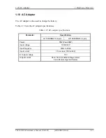
Reviews: