GND
SDI
CLK
LE(ED1)
OUT0
OUT1
OUT2
OUT3
OUT4
OUT5
OUT6
OUT7
OE(ED2)
SDO
R-EXT
VDD
VIA to GND
To
µC
To
µC
To
µC
To
µC
To
µC
VDD
VLED
SLVS695D – JUNE 2007 – REVISED JANUARY 2015
11 Power Supply Recommendations
The device is designed to operate from a VDD supply between 3 V and 5.5 V. The LED supply voltage is
determined by the number of LEDs in each string and the forward voltage of the LEDs.
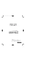
12 Layout
12.1 Layout Guidelines
The traces that carry current from the LED cathodes to the OUTx pins must be wide enough to support the
default current (up to 120 mA).
The SDI, CLK, LE (ED1), OE (ED2), and SDO pins are to be connected to the microcontroller. There are several
ways to achieve this, including the following methods:
•
Traces may be routed underneath the package on the top layer.
•
The signal may travel through a via to another layer.
12.2 Layout Example
Figure 24. PW Package Layout
Copyright © 2007–2015, Texas Instruments Incorporated
27
Product Folder Links: