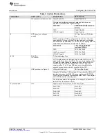


Green
1
2
D5
MSP_LED
270
R14
1
2
3
Q1
BSS138
VBUS
D_N
D_P
0.1µF
C1
33
0402
R1
33
0402
R3
1.2Meg
R7
220pF
C11
1
2
3
4
S1
BSL
1.5k
0402
R4
PUR
VUSB
220pF
C17
7.5V
D1
1SMB5922BT3G
22µF
0805
C5
10µF
C2
10µF
C3
U2A_3V3
P6.4/CB4/A4
1
P6.5/CB5/A5
2
P6.6/CB6/A6
3
P6.7/CB7/A7
4
P7.0/CB8/A12
5
P7.1/CB9/A13
6
P7.2/CB10/A14
7
P7.3/CB11/A15
8
P5.0/A8/VREF+/VEREF+
9
P5.1/A9/VREF-/VEREF-
10
AVCC1
11
P5.4/XIN
12
P5.5/XOUT
13
AVSS1
14
P8.0
15
P8.1
16
P8.2
17
DVCC1
18
DVSS1
19
VCORE
20
P1.0/TA0CLK/ACLK
21
P1.1/TA0.0
22
P1.2/TA0.1
23
P1.3/TA0.2
24
P1.4/TA0.3
25
P1.5/TA0.4
26
P1.6/TA1CLK/CBOUT
27
P1.7/TA1.0
28
P2.0/TA1.1
29
P2.1/TA1.2
30
P2.2/TA2CLK/SMCLK
31
P2.3/TA2.0
32
P2.4/TA2.1
33
P2.5/TA2.2
34
P2.6/RTCCLK/DMAE0
35
P2.7/UCB0STE/UCA0CLK
36
P3.0/UCB0SIMO/UCB0SDA
37
P3.1/UCB0SOMI/UCB0SCL
38
P3.2/UCB0CLK/UCA0STE
39
P3.3/UCA0TXD/UCA0SIMO
40
P3.4/UCA0RXD/UCA0SOMI
41
P3.5/TB0.5
42
P3.6/TB0.6
43
P3.7/TB0OUTH/SVMOUT
44
P4.0/PM_UCB1STE/PM_UCA1CLK
45
P4.1/PM_UCB1SIMO/PM_UCB1SDA
46
P4.2/PM_UCB1SOMI/PM_UCB1SCL
47
P4.3/PM_UCB1CLK/PM_UCA1STE
48
DVSS2
49
DVCC2
50
P4.4/PM_UCA1TXD/PM_UCA1SIMO
51
P4.5/PM_UCA1RXD/PM_UCA1SOMI
52
P4.6/PM_NONE
53
P4.7/PM_NONE
54
P5.6/TB0.0
55
P5.7/TB0.1
56
P7.4/TB0.2
57
P7.5/TB0.3
58
P7.6/TB0.4
59
P7.7/TB0CLK/MCLK
60
VSSU
61
PU.0/DP
62
PUR
63
PU.1/DM
64
VBUS
65
VUSB
66
V18
67
AVSS2
68
P5.2/XT2IN
69
P5.3/XT2OUT
70
TEST/SBWTCK
71
PJ.0/TDO
72
PJ.1/TDI/TCLK
73
PJ.2/TMS
74
PJ.3/TCK
75
RST/NMI/SBWTDIO
76
P6.0/CB0/A0
77
P6.1/CB1/A1
78
P6.2/CB2/A2
79
P6.3/CB3/A3
80
U4
MSP430F5529IPN
0.1µF
C21
0.1µF
C20
0.1µF
C19
U2A_3V3
PUR
U2A_3V3
0.47µF
C18
VBUS
VUSB
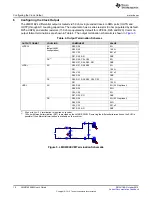
USER NOTE:
Features not supported by On-board or External USB2ANY circuiry
- Sw3.3V_EXT supply
- Sw5V_EXT supply
- ADCs 0-4
- DACs 0-1
- PWMs 0-3
- SPI interface (I2C/SMBus only)
I2CPU
V18
EXT5V_EN
EXT5V_FAULT
EXT3.3V_EN
EXT3.3V_FAULT
0.1µF
C15
100k
R16
2200pF
C16
33k
R15
U2A_3V3
D_N
D_P
1
2
24MHz
Y1
ECS-240-20-5PX-TR
33k
R5
VCORE
SDA
SCL
0 R10
0 R11
U2A_GPIO4
U2A_GPIO5
0 R12
0 R13
USER NOTE:
De-populate the 0-ohm resistors connected to "U2A_GPIOx" and "U2A_3V3"
nets before attaching the External USB2ANY module to the USB2ANY Header.
LAYOUT NOTE:
Place 0-ohm footprints close to USB2ANY Header pins to minimize trace stubs
when 0-ohm resistors are de-populated (to disconnect the on-board MSP430).
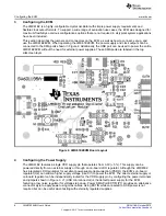
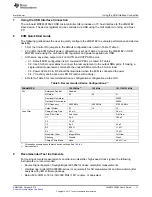
3.3 V, 150 mA REGULATOR FOR USB2ANY
USB MINI-B CONNECTOR
ON-BOARD USB2ANY/MSP430
VBUS_FILT
33k
R2
0.1µF
C9
VIN
1
GND
2
EN
3
N/C
4
VOUT
5
U2
LP5907MFX-3.3/NOPB
33k
R6
0.1µF
C12
20V
D2
B220A-13-F
10µF
C6
1µF
C7
0.1µF
C8
GND
GND
GND
GND
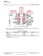
EXTIN
SH1_2_3
VDD
EXTIN
SH2_2_3
VDD_REG
VBUS_FILT
3.3 V, 250 mA REGULATOR FOR LMK61XX
Green
1
2
D3
VDD
I=
5
m
A
SDA
SCL
U2A_GPIO2
U2A_GPIO3
U2A_GPIO4
U2A_GPIO5
U2A_GPIO6
U2A_GPIO7
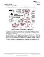
J7 connects to J5 of USB2ANY module via Ribbon cable
USB2ANY HEADER (VERTICAL)
SCL
SDA
2
3
4
1
5
J1
1734035-2
60 ohm
FB1
1
2
3
4
5
6
7
8
9
10
J4
DNP
TP2
TP3
1
2
3
4
5
P1
EXTIN
SH4_2_3
1.5k
R17
1.5k
R19
VDD
GND
OE
SH3_2_3
1.5k
R18
1.5k
R20
VDD
GND
ADD
OE / ADD JUMPERS
1µF
C10
1µF
C4
1
2
3
J5
OE
1
2
3
J6
ADD
1
2
3
J2
REG SUP
1
2
3
J3
IC SUP
1
1
LABEL SW: BSL
LABEL PINS:
1 = SDA
2 = SCL
5 = GND
6 = 3.3V
8 = OE
10 = ADD
LABEL PINS:
1 = GND
2 = <JP NAME>
3 = VDD
4 = U2A
LABEL PINS:
1 = GND
2 = <JP NAME>
3 = VDD
4 = U2A
LAYOUT NOTE:
Place C10 and C4 on the same side as U
and as close to the package as possible. Use
wide and short traces.
LAYOUT NOTE:
Place LED on L1, other components can be on L4
VDD
510
R8
Orange
1
2
D4
I2C
270
R9
U2A_3V3
U2A_GPIO5
U2A_GPIO4
30pF
C13
30pF
C14
USB_N
USB_P
IO
1
1
IO
2
2
G
N
D
3
IO
3
4
IO
4
5
VC
C
6
U3
TPD4E004DRYR
IN
6
OUT
1
GND
3
EN
4
NC
5
DAP
7
NC
2
U1
LP5900SD-3.3/NOPB
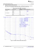
EVM Schematic
19
SNAU188 – October 2015
LMK61E2EVM User's Guide
Copyright © 2015, Texas Instruments Incorporated


