


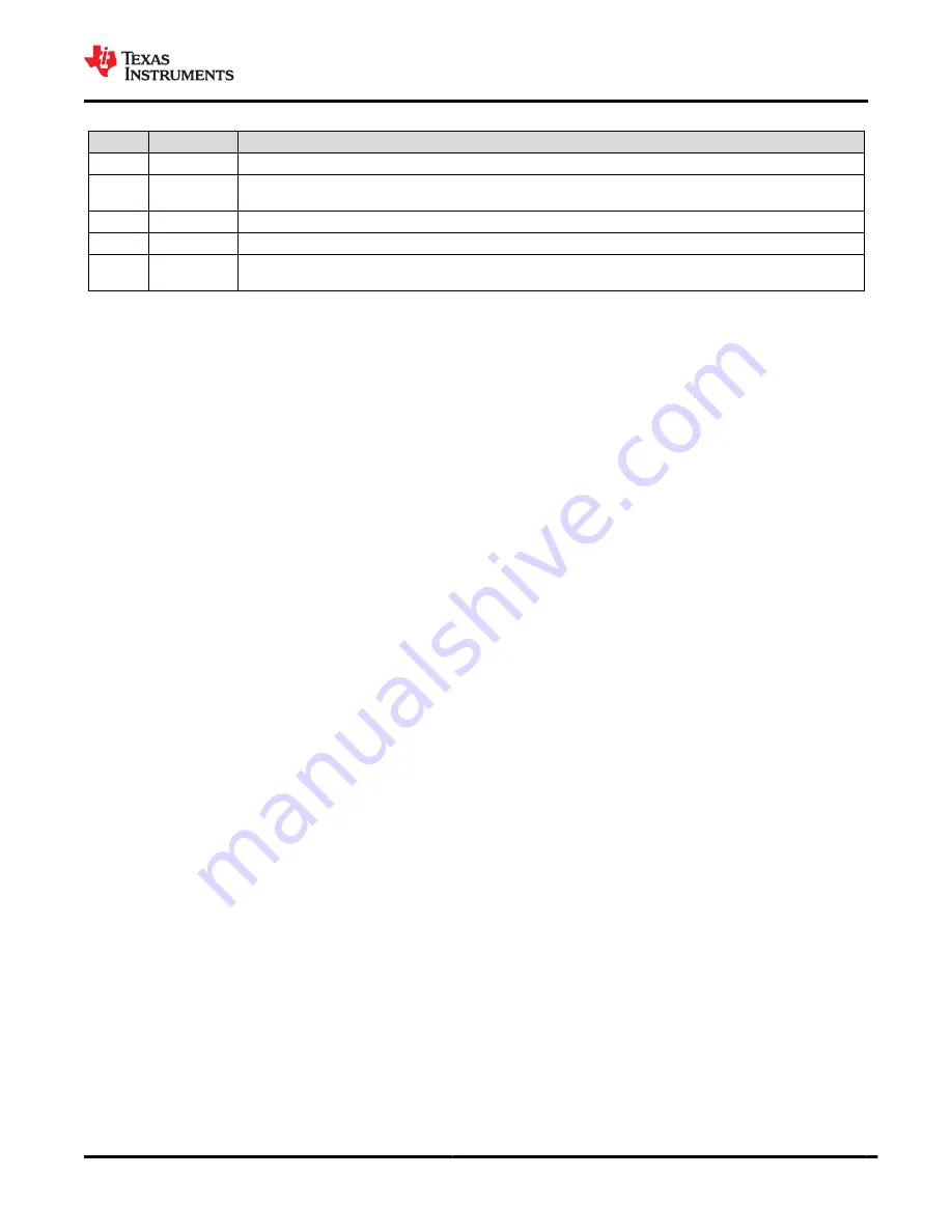
Table 16-3. Terminating Unused Pins (continued)
Pin
Name
Recommendation
40
PCHG
If not used, this pin should be left floating.
41
LD
If the DSG driver is not used, this pin can be connected through a series resistor to the PACK+ connector or can
be connected to pin 17 (VSS).
43
DSG
If not used, this pin should be left floating.
45
CHG
If not used, this pin should be left floating.
46
CP1
If not used, this pin should be connected to pin 47 (BAT). Note: If the charge pump is enabled with CP1
connected to BAT, the device consumes an additional ≈200 µA.
17 Power Supply Requirements
The BQ76942 device draws its supply current from the BAT pin, which is typically connected to the top of stack
point through a series diode, to protect against any fault within the device resulting in unintended charging of the
pack. A series resistor and capacitor is included to lowpass filter fast variations on the stack voltage. During a
short circuit event, the stack voltage may be momentarily pulled to a very low voltage before the protection FETs
are disabled. In this case, the charge on the BAT pin capacitor will temporarily support the BQ76942 device
supply current, to avoid the device losing power.
18 Layout
18.1 Layout Guidelines
• The quality of the Kelvin connections at the sense resistor is critical. The sense resistor must have
a temperature coefficient no greater than 50 ppm in order to minimize current measurement drift with
temperature. Choose the value of the sense resistor to correspond to the available overcurrent and short-
circuit ranges of the BQ76942 device. Parallel resistors can be used as long as good Kelvin sensing is
ensured. The device is designed to support a 1-mΩ sense resistor.
• In reference to the system circuitry, the following features require attention for component placement and
layout: Differential Low-Pass Filter, and I
2
C communication.
• The BQ76942 device uses an integrating delta-sigma ADC for current measurements. For best performance,
100-Ω resistors should be included from the sense resistor terminals to the SRP and SRN inputs of the
device, with a 0.1-μF filter capacitor placed across the SRP and SRN pins. Optional 0.1-µF filter capacitors
can be added for additional noise filtering at each sense input pin to ground. All filter components should
be placed as close as possible to the device, rather than close to the sense resistor, and the traces from
the sense resistor routed in parallel to the filter circuit. A ground plane can also be included around the filter
network to add additional noise immunity.
• The BQ76942 device internal REG18 LDO requires an external decoupling capacitor, which should be placed
as close to the REG18 pin as possible, with minimized trace inductance, and connected to a ground plane
electrically connected to VSS.
• The I
2
C clock and data pins have integrated ESD protection circuits; however, adding a Zener diode and
series resistor on each pin provides more robust ESD performance.
18.2 Layout Example
An example circuit layout using the BQ76942 device in a 7-series cell design is described below. The design
implements the schematic shown in
, and uses a 2.5-inch × 2.75-inch 2-layer circuit
card assembly, with cell connections on the left edge, and pack connections along the top edge of the board.
Wide trace areas are used, reducing voltage drops on the high current paths.
The board layout, which is shown in
and
, includes spark gaps with the reference
designator prefix
E
. These spark gaps are fabricated with the board, and no component is installed.
SLUSE14B – DECEMBER 2020 – REVISED DECEMBER 2021
Copyright © 2021 Texas Instruments Incorporated
75
Product Folder Links:
Summary of Contents for BQ76942
Page 84: ......


