background image

S

UPER S2DM3/S2DME User's


Manual

1-6

Introduction

COM2

COM1

  J14

  J13

J13

PS/2  KB

PS/2  MOUSE

  J10

  J8

J12

USB

ULTRA WIDE SCSI

  BT1

BATTERY

J22

Parallel

Port

  J11

FLO

P

PY

12.5"

      12"

PCI 1

PCI 2

PCI 3

PCI 4

ATX POWER

CPU 1

FAN

  J48

®

  WOL

PCI64 #2 (3.3V)

PCI64 #1 - SISL (3.3V)

  J9

AGP PRO

CPU 2

FAN

THRM

FAN

B

ank0

B

ank2

B

ank3

B

ank1

  PWR_SEC

Ch FAN 1 Ch FAN 2

ID

E

 #1

ID

E #2

  WOR

  JBT1

1

1

  JP7

  JP5

1

  JP3

S

UPER     S2DM3

ULTRA III LVD/SE

FWH
(BIOS)

  J34

  J15  J14

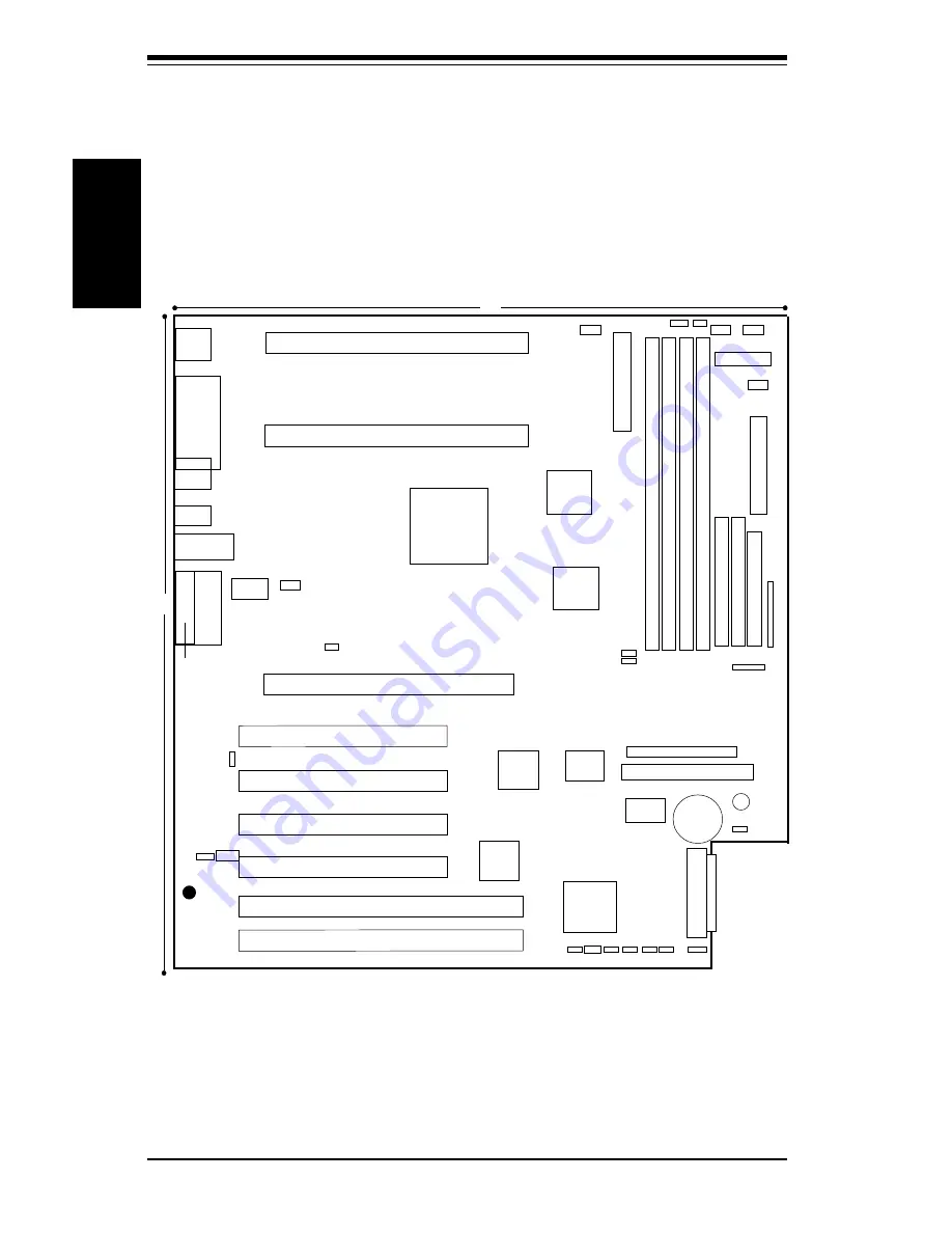
Figure 1-3.  SUPER S2DM3 Layout

(not drawn to scale)

  IR Header

  JF1

LINE IN

LINE OUT

MIC

GAME

PORT

  J28

  JA2

  JA6

  JP13

  JP12

  JP4

  JP10

  JP11

  JA1

  JL1

1

Also see the figure on page 2-6 for the locations of the I/O ports and
2-7 for the Front Control Panel (JF1) connectors.

  J38
Ethernet

1

1

  SLED

  BZ1

  J44

CPU 1

CPU 2

  J16

ATX POWER

  J27

50-pin SCSI

  JA5

Summary of Contents for SUPER S2DM3

Page 1: ...SUPER S2DM3 SUPER S2DME USER S MANUAL Revision 1 0 SUPER...

Page 2: ...ILITY TO USE THIS PRODUCT OR DOCUMENTATION EVEN IF ADVISED OF THE POSSIBILITY OF SUCH DAMAGES IN PARTICULAR THE VENDOR SHALL NOT HAVE LIABILITY FOR ANY HARDWARE SOFTWARE OR DATA STORED OR USED WITH TH...

Page 3: ...the processor and DIMM memory mod ules and when mounting the mainboard in the chassis Also refer to this chapter to connect the floppy and hard disk drives SCSI drives the IDE interfaces the parallel...

Page 4: ...iv SUPER S2DM3 S2DME User s Manual Notes...

Page 5: ...1 1 2 Chipset Overview 1 13 1 3 PC Health Monitoring 1 14 1 4 ACPI PC 98 Features 1 16 1 5 Power Supply 1 18 1 6 Super I O 1 19 Chapter 2 Installation 2 1 Static Sensitive Devices 2 1 Precautions 2 1...

Page 6: ...ED Indicator 2 14 2 7 Jumper Settings 2 14 Explanation of Jumpers 2 14 CMOS Clear 2 14 Front Side Bus Speed 2 15 AC 97 Enable Disable 2 15 SCSI Termination Enable Disable 2 15 Overheat Alarm Enable Di...

Page 7: ...S Features 4 2 4 3 Running Setup 4 2 Standard CMOS Setup 4 4 Advanced CMOS Setup 4 5 Advanced Chipset Setup 4 9 Power Management 4 11 PCI Plug and Play Setup 4 14 Peripheral Setup 4 17 Auto Detect Har...

Page 8: ...Notes SUPER S2DM3 S2DME User s Manual...

Page 9: ...l been included with your motherboard If anything listed here is damaged or missing contact your retailer One 1 Supermicro Mainboard One 1 ATA66 ribbon cable for IDE devices One 1 Floppy ribbon cable...

Page 10: ...SUPER S2DM3 S2DME User s Manual 1 2 Introduction Notes...

Page 11: ...E mail marketing supermicro com General Information support supermicro com Technical Support Web site www supermicro com European Office Address Super Micro Computer B V Het Sterrenbeeld 28 5215 ML s...

Page 12: ...SUPER S2DM3 S2DME User s Manual 1 4 Introduction SUPER S2DM3 Figure 1 1 SUPER S2DM3 Image...

Page 13: ...Chapter 1 Introduction 1 5 Introduction SUPER S2DME Figure 1 2 SUPER S2DME Image shares the same PCB with the S2DM3 but without SCSI...

Page 14: ...FAN Bank0 Bank2 Bank3 Bank1 PWR_SEC Ch FAN 1 Ch FAN 2 IDE 1 IDE 2 WOR JBT1 1 1 JP7 JP5 1 JP3 S UPER S2DM3 ULTRA III LVD SE FWH BIOS J34 J15 J14 Figure 1 3 SUPER S2DM3 Layout not drawn to scale IR Hea...

Page 15: ...Device Header p 2 11 Bank0 Bank3 Memory RAM Slots p 2 5 J12 Universal Serial Bus Ports p 2 12 J13 PS 2 Keyboard Mouse p 2 12 J14 J15 IDE Hard Disk Drive Connectors p 2 18 J16 Floppy Disk Drive Connect...

Page 16: ...PS 2 MOUSE J10 J8 J12 USB BT1 BATTERY J22 Parallel Port J11 FLOPPY 12 5 12 PCI 1 PCI 2 PCI 3 PCI 4 ATX POWER CPU 1 FAN J48 WOL PCI64 2 3 3V PCI64 1 SISL 3 3V J9 AGP PRO CPU 2 FAN THRM FAN Bank0 Bank2...

Page 17: ...GAME Game Port IR Header Infrared Device Header p 2 11 Bank0 Bank3 Memory RAM Slots p 2 5 J12 Universal Serial Bus Ports p 2 12 J13 PS 2 Keyboard Mouse p 2 12 J14 J15 IDE Hard Disk Drive Connectors p...

Page 18: ...1 5 840 Chipset System Block Diagram MCH Pentium III II Xeon CPU ICH 241 BGA 133 100 MHz Host Bus 33 MHz PCI Slots USB BIOS 4Mb FWH AGP Pro SuperI O LPC 1 5 Mb sec AC 97 AGP 2 0 Pentium III II Xeon CP...

Page 19: ...MHz PCI slots Four 32 bit 33 MHz PCI slots 1 AGP Pro slot BIOS 4 Mb Firmware Hub AMI Flash BIOS APM 1 2 DMI 2 1 PCI 2 2 ACPI 1 0 Plug and Play PnP PC Health Monitoring Five onboard voltage monitors f...

Page 20: ...2 Fast UART 16550A compatible serial ports 1 EPP Enhanced Parallel Port and ECP Extended Capabilities Port supported parallel port PS 2 mouse and PS 2 keyboard ports 1 infrared port 2 USB Universal S...

Page 21: ...4x fast write capa bility and operates at a peak bandwidth of 266 MB sec The MCH host interface bus runs at 133 100 MHz I O Controller Hub ICH The ICH is the Controller Hub for the I O subsystem and i...

Page 22: ...only AOL2 ASIC brings an advanced level of management interface between a remote management console server and the client system It provides inter faces to the 82559 Ethernet controller chip and to sy...

Page 23: ...enever the CPU temperature exceeds a user defined threshold The overheat circuitry runs independently from the CPU It can continue to monitor for overheat conditions even when the CPU is in sleep mode...

Page 24: ...ced Configuration and Power Interface The ACPI specification defines a flexible and abstract hardware interface that pro vides a standard way to integrate power management features throughout a PC sys...

Page 25: ...d will work like a normal keyboard during system boot up Real Time Clock Wake Up Alarm Although the PC may be perceived to be off when not in use it is still capable of responding to preset wake up ev...

Page 26: ...ove compliant power supply 1 5 Power Supply As with all computer products a stable power source is necessary for proper and reliable operation It is even more important for processors that have high C...

Page 27: ...h supports serial infrared communication Each UART includes a 16 byte send receive FIFO a programmable baud rate generator complete modem control capability and a processor interrupt sys tem Both UART...

Page 28: ...SUPER S2DM3 S2DME User s Manual 1 20 Introduction Notes...

Page 29: ...al object before removing the board from the antistatic bag Handle the board by its edges only do not touch its components peripheral chips memory modules or gold contacts When handling chips or modul...

Page 30: ...ired for mounting the DRM Dual Retention Module See Figure 2 1 for mounting hole locations 2 Mounting the motherboard onto the motherboard tray Except for the four Slot 2 mounting holes use a Philips...

Page 31: ...e of the installation process When removing the Pentium II III processor avoid press ing down on the motherboard or components Extra for Slot 2 Figure 2 1 Dual Retention Module Mounting holes ATX Stan...

Page 32: ...ifferent types of chassis Chassis may include a variety of mounting fasteners made of metal or plastic Although a chassis may have both types metal fasteners are the most highly recommended because th...

Page 33: ...he module to prevent inserting the DIMM module incorrectly 3 Gently press down on the DIMM module until it snaps into place in the slot As stated in 1 above you must populate either two or four banks...

Page 34: ...rt Control Panel Connector Locations The I O ports are color coded in conformance with the PC 99 specification See Figure 2 4 below for the colors and locations of the various I O ports Parallel Port...

Page 35: ...s header pins for various front control panel connectors See Figure 2 5 for the pin definitions of the speaker overheat LED keyboard lock chassis intrusion I2 C USB0 reset power on hard drive LED and...

Page 36: ...V 20 5V Secondary Power Connector Use of the Secondary Power con nector PWR_SEC is recom mended when a heavy load of pe ripherals has been added to the motherboard Note Be sure to use a 6 pin connecto...

Page 37: ...itions JF1 Reset The Reset connection is located on pins 15 and 17 of JF1 This connector attaches to the hard ware reset switch on the com puter case See Table 2 7 for pin definitions Pin Number 15 17...

Page 38: ...onnect an LED to the OH connec tion on pin 26 of JF1 to provide advanced warning of chassis overheating Refer to Table 2 11 for pin definitions Pin Number 10 Definition OH Active Table 2 11 Overheat L...

Page 39: ...rt See Table 2 16 for pin definitions Table 2 16 Serial Port Pin Definitions COM1 COM2 Pin Number Definition 1 DCD 2 DSR 3 Serial In 4 RTS 5 Serial Out Pin Number Definition 6 CTS 7 DTR 8 RI 9 Ground...

Page 40: ...rd and Mouse Port Pin Definitions J13 Pin Number 1 2 3 4 5 6 Definition Data NC Ground VCC Clock NC CD Headers There are two CD headers of dif ferent sizes on the motherboard to enable audio CD playba...

Page 41: ...nd keyboard will be disabled but no audible alarm will be activated All system opera tions will halt until the intrusion microswitch is set back to normal See Table 2 22 for pin definitions Pin Number...

Page 42: ...l CMOS Clear Position 1 2 Position 2 3 Normal CMOS Clear 2 7 Jumper Settings Explanation of Jumpers To modify the operation of the moth erboard jumpers can be used to choose between optional settings...

Page 43: ...Enable Disable Jumper Settings JA1 Overheat Alarm Enable Disable You may want to disable the audio alarm signal that notifies you of over temperature condtions Jumper JP10 gives you this option If dis...

Page 44: ...e Disable Jumper Settings JP11 Power Supply Failure Alarm Enable Disable The system will notify you in the event of a power supply failure This feature assumes that three power supply units are instal...

Page 45: ...DIN 4 Reserved 6 FDEDIN 8 Index 10 Motor Enable 12 Drive Select B 14 Drive Select A 16 Motor Enable 18 DIR 20 STEP 22 Write Data 24 Write Gate 26 Track 00 28 Write Protect 30 Read Data 32 Side 1 Selec...

Page 46: ...s flush with the edge of the motherboard the card should be inserted correctly AGP Pro Slot Edge of motherboard IDE Connectors There are no jumpers to config ure the onboard IDE connectors J14 and J15...

Page 47: ...able 2 36 for pin definitions for the 50 pin Legacy SCSI con nector located at JA6 Pin Number Function 1 GND 2 GND 3 GND 4 GND 5 GND 6 GND 7 GND 8 GND 9 GND 10 GND 11 GND 12 GND 13 GND 14 GND 15 GND 1...

Page 48: ...24 25 26 27 28 29 30 31 32 33 34 Signal Names DB 12 DB 13 DB 14 DB 15 DB P1 DB 0 DB 1 DB 2 DB 3 DB 4 DB 5 DB 6 DB 7 DB P GROUND GROUND TERMPWR TERMPWR RESERVED GROUND ATN GROUND BSY ACK RST MSG SEL C...

Page 49: ...click on the S Setup icon Figure 2 6 Driver Tool Installation Display Screen Click the icons showing a hand writing on paper to view the readme files for each item Click the tabs to the right of these...

Page 50: ...2 22 SUPER S2DM3 S2DME User s Manual Installation Notes...

Page 51: ...hose for the keyboard and mouse 3 Remove all add on cards 4 Install a CPU making sure it is fully seated and connect the chassis speaker and the power LED to the motherboard Check all jumper settings...

Page 52: ...o end users so it is best to first check with your distributor or reseller for troubleshooting services They should know of any possible problem s with the specific system configuration that was sold...

Page 53: ...echnical support department We can be reached by e mail at support supermicro com or by fax at 408 895 2012 3 3 Frequently Asked Questions Question What are the various types of memory that the S2DM3...

Page 54: ...o How can I correct this Answer If the system does not have video after flashing your new BIOS it indicates that the flashing procedure failed To remedy this first clear CMOS per the instructions in t...

Page 55: ...my microphone correctly but I can t record any sound What should I do Answer Go to Start Programs Accessories Entertainment and then Volume Control Under the Properties tab scroll down the list of de...

Page 56: ...turning to the manufacturer the RMA number should be prominently displayed on the outside of the shipping carton and mailed prepaid or hand carried Ship ping and handling charges will be applied for a...

Page 57: ...omputer is turned off The original IBM AT had 64 kbytes of non volatile memory storage in CMOS RAM All AT compatible systems have at least 64 kbytes of CMOS RAM which is usually part of the Real Time...

Page 58: ...h Monitoring chips When a failure occurs in a monitored activity AMIBIOS can sound an alarm and display a message The PC Health Monitoring chips monitor CPU temperature Additional temperature sensors...

Page 59: ...ector Virus Protection Disabled Month Jan Dec ESC Exit Sel Day 01 31 PgUp PgDn Modify Year 1901 2099 F2 F3 Color AMIBIOS HIFLEX SETUP UTILITY VERSION 1 18 1998 American Megatrends Inc All Rights Reser...

Page 60: ...n with a list of drive parameters appears Click on OK to configure the drive Type How to Configure SCSI Select Type Select Not Installed on the drive parameter screen The SCSI drivers provided by the...

Page 61: ...per track SCSI and IDE drive may have even more sectors per track Capacity The formatted capacity of the drive is Number of heads x Number of cylinders x Number of sectors per track x 512 bytes per se...

Page 62: ...evice 3rd Boot Device The options for the 1st Boot Device are Disabled 1st IDE HDD 2nd IDE HDD 3rd IDE HDD 4th IDE HDD Floppy ARMD FDD ARMD HDD ATAPI CDROM SCSI Network or I2 0 The options for the 2nd...

Page 63: ...option are BIOS or Silent If selected as BIOS the POST will start with the normal sign on message screen If Silent is selected the POST will start with the Supermicro screen Display Mode at Add On ROM...

Page 64: ...he system boots or the end user runs WinBIOS Setup If Always is chosen a user password prompt appears every time the computer is turned on If Setup is chosen the password prompt appears if WinBIOS Set...

Page 65: ...r all settings except C000 and C400 which are Cached for default When set to Disabled the contents of the video ROM are not copied to RAM When set to Enabled the contents of the video ROM area from C0...

Page 66: ...ortion of memory for ISA cards DMA 0 Type DMA 1 Type DMA 2 Type DMA 3 Type DMA 5 Type DMA 6 Type DMA 7 Type These options determine the bus that the specified DMA channel can be used on The settings a...

Page 67: ...he settings for this option are S1 and C2 S1 is a normal suspend state in which no system CPU or chipset context is lost C2 is a low power state In this state the system cache is maintained Standby Ti...

Page 68: ...default setting for this option is Standby and the Fail Safe default setting is Disabled Hard Disk Time Out Minutes This option specifies the length of a period of hard disk drive inactivity When thi...

Page 69: ...ngs for this option are Enabled and Disabled TCO Logic SMI Enable This allows the TCO logic to generate a System Management Interrupt when a century rollover occurs The settings are Enabled and Dis ab...

Page 70: ...me This allows you to wake up the system from a system management bus device The settings for this option are Enabled and Disabled LAN Wake Up This allows you to make use of the Wake on LAN feature Th...

Page 71: ...lette registers This will permit the palette registers of both devices to be identical This option must be set to Enabled if any ISA adapter card installed in the system requires VGA palette snooping...

Page 72: ...channels control the data transfers between the I O devices and the system memory The chipset allows the BIOS to choose which channels to do the job The settings are PnP or ISA EISA IRQ3 IRQ4 IRQ5 IR...

Page 73: ...Setup Onboard SCSI This setting enables or disables the onboard SCSI non applicable to the PIIIDME The settings are Enabled and Disabled CPU1 Current Temperature The current temperature of CPU1 is di...

Page 74: ...he settings are Disabled 3F8h 2F8h 3E8h and 2E8h Serial Port2 Mode The settings for this option are Normal IrDA SIR A IrDA SIR B ASKIR Consumer and Raw IR When set to anything but Normal the IR Duplex...

Page 75: ...Parallel Port ECP DMA Channel This option is only available if the setting of the parallel port mode option is ECP The settings are 0 1 2 3 5 6 and 7 Onboard MIDI Port This option specifies the base...

Page 76: ...rvisor or User password AMIBIOS prompts you for the new password You must set the Supervisor password before you can set the User password Enter a 1 6 character password It will not appear on the scre...

Page 77: ...this and hit Enter when you wish to save any changes made to settings in BIOS and exit back to the system boot up procedure Exit Without Saving Highlight this and hit Enter when you wish to exit back...

Page 78: ...SUPER S2DM3 S2DME Manual 4 22 BIOS Notes...

Page 79: ...he screen Fatal errors are those which will not allow the system to continue the boot up procedure If a fatal error occurs you should consult with your system manufacturer for possible repairs These f...

Page 80: ...d an error 6 8042 Gate A20 Failure The keyboard controller 8042 contains the Gate A20 switch which allows the CPU to operate in virtual mode This error means that the BIOS cannot switch the CPU into p...

Page 81: ...r replace the keyboard fuse if the keyboard has one 8 times there is a memory error on the video adapter Replace the video adapter or the RAM on the video adapter 9 times the BIOS ROM chip is bad The...

Page 82: ...ache CH 2 Timer Error Most ISA computers include two times There is an error in time 2 CMOS Battery State Low CMOS RAM is powered by a battery The battery power is low Replace the battery CMOS Checksu...

Page 83: ...and follow the screen instructions Display Switch Some compters require a video switch on the Not Proper motherboard be set to either color or monochrome Turn the computer off set the switch then pow...

Page 84: ...nnector No ROM BASIC Cannot find a bootable sector on either disk drive A or hard disk drive C The BIOS calls INT 18h which generates this message Use a bootable disk Off Board Parity error in memory...

Page 85: ...isabling cache memory 06 Uncompressing the post code unit next 07 Next initializing the CPU init and the CPU data area 08 The CMOS checksum calculation is done next 0B Next performing any required ini...

Page 86: ...e chipset 14 The 8254 timer test will begin next 19 The 8254 timer test is over Starting the memory refresh test next 1A The memory refresh test line is toggling Checking the 15 second on off time nex...

Page 87: ...control to BIOS POST Performing any required processing after the video ROM had control 2E Completed post video ROM test processing If the EGA VGA controller is not found performing the display memor...

Page 88: ...nd at 0 0 next 45 Data initialized Checking for memory wraparound at 0 0 and finding the total system memory size next 46 The memory wraparound test has completed The memory size calculation has been...

Page 89: ...zed Adjusting the displayed memory size for relocation and shadowing next 51 The memory size display was adjusted for relocation and shadowing Testing the memory above 1 MB next 52 The memory above 1...

Page 90: ...learing the output buffer and checking for stuck keys Issuing the keyboard reset command next 81 A keyboard reset error or stuck key was found Issuing the keyboard controller interface test command ne...

Page 91: ...PS 2 mouse check and extended BIOS data area allocation check next 8C Programming the WINBIOS Setup options next 8D The WINBIOS Setup options are programmed Resetting the hard disk controller next 8F...

Page 92: ...red initialization after the Coprocessor test next 9E Initialization after the Coprocessor test is complete Checking the extended keyboard keyboard ID and Num Lock key next Issuing the keyboard ID com...

Page 93: ...elay is starting Next the initialization cade checksum will be verified D1h Initializing the DMA controller Performing the keyboard controller BAT test Starting memory refresh and entering 4 GB flat m...

Page 94: ...SUPER S2DM3 S2DME Manual B 10 APPENDIX B Notes...

Reviews: