1-4
C2SBM-Q User’s Manual
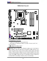
Motherboard Layout
Important Notes to the User
• Jumpers not indicated are for test purposes only.
• See Chapter 2 for detailed information on jumpers, I/O ports and JF1 front
panel connections.
• " " indicates the location of "Pin 1.'
Overclocking Considerations
Warning:
Please be aware of the following conditions when "overclocking" is
used:
Setting a high CPU FSB speed (overclocking), DRAM frequency or se-
lecting a high CPU V-Core voltage, memory voltage, chipset voltage, ICH chipset
voltage, or FSB termination voltage may result in system instability. If this occurs,
revert to the default settings. In addition, extra fans may be needed for proper system
cooling. The C2SBM-Q offers the option of "overclocking" however, Supermicro is
not responsible for any damage caused by the use of overclocking.
FA
N
1
JI2C2
JWOR
JFSB3
JF1
JWD
JLED
Battery
J40
DI
M
M
1A
DI
M
M
2A
DI
M
M
1B
I-SATA2
I-SATA3
SPEAKER
KB
/M
OU
SE
CPU Fan
J28
VG
A
JGS1
US
B
2/3
/4/
5
J43
J11
US
B 0
,1
J46
Au
dio
J41
4-Pin PWR
LGA 775 CPU
JFSB2
JFSB1
PC
I2
Slot5 PCI-E x4
JPAC
J9
Buzzer
SPKR
Slot4 PCI-33MHz
PC
I1
J1
2
J3
IDE#1
J4
5
FP USB 8/9
FP USB 6/7
J4
4
JL1
LE1
FP
CT
RL
Intel Q35
24
-pi
n A
TX
P
W
R
Audio CTRL
CD-IN
CD1
Front Audio
W
83
62
7D
HG
S
I/O
1
IDE CTRL
ITE 8213
J15
COM4
USB 10
JWOL
I-SATA0
I-SATA1
JS
4
JS
3
JS
1
JS
2
FA
N2
Fa
n3
JPUSB1
PC
I3
Slot7 PCI-E x16
JI2C1
JP2
Intel ICH9DO
JPUSB2
J4
7
JPL1
CO
M2
W
83
62
7D
HG
S
I/O
2
J14
COM3
Slot6 PCI-33MHz
PC
I1
JPT1
DI
M
M
2B
LAN CTRL
LA
N
1
C2
SB
M-
Q
CO
M1
J31
JBT1
!
Summary of Contents for C2SBM-Q
Page 1: ...C2SBM Q USER S MANUAL Revision 1 1a...
Page 52: ...3 6 C2SBM Q User s Manual Notes...
Page 78: ...4 26 C2SBM Q User s Manual Notes...
Page 84: ...A 6 C2SBM Q User s Manual Notes...
Page 90: ...B 6 C2SBM Q User s Manual Notes...


