2-12
C2SBM-Q User's Manual
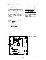
Power Button
OH/Fan Fail LED
1
NIC1 LED
Reset Button
2
HDD LED
Power LED
Reset
PWR
LE
LE
LE
LE
Ground
Ground
X
X
X
X
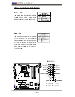
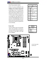
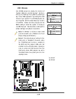
Power Button
The Power Button connection is located
on pins 1 and 2 of JF1. Momentarily con-
tacting both pins will power on/off the sys-
tem. This button can also be configured
to function as a suspend button (with a
setting in the BIOS - see Chapter 4). To
turn off the power when set to suspend
mode, press the button for at least 4
seconds. Refer to the table on the right
for pin definitions.
Note:
Do not close or short Pins 1
& 2 since this will cause the system
to continuously reboot.
Power Button
Pin Definitions (JF1)
Pin# Definition
1
Signal
2
+3V Standby
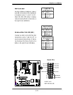
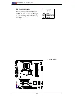
Reset Button
The Reset Button connection is located
on pins 3 and 4 of JF1. Attach it to a
hardware reset switch on the computer
case. Refer to the table on the right for
pin definitions.
Reset Button
Pin Definitions (JF1)
Pin# Definition
3
Reset
4
Ground
A.
Reset
B.
PWR Button
Header Pins
B
A
FA
N
1
JI2C2
JWOR
JFSB3
JF1
JWD
JLED
Battery
J40
DI
M
M
1A
DI
M
M
2A
DI
M
M
1B
I-SATA2
I-SATA3
SPEAKER
KB
/M
OU
SE
CPU Fan
J28
VG
A
JGS1
US
B
2/3
/4/
5
J43
J11
US
B 0
,1
J46
Au
dio
J41
4-Pin PWR
LGA 775 CPU
JFSB2
JFSB1
PC
I2
Slot5 PCI-E x4
JPAC
J9
Buzzer
SPKR
Slot4 PCI-33MHz
PC
I1
J1
2
J3
IDE#1
J4
5
FP USB 8/9
FP USB 6/7
J4
4
JL1
LE1
FP
CT
RL
Intel Q35
24
-pi
n A
TX
P
W
R
Audio CTRL
CD-IN
CD1
Front Audio
W
83
62
7D
HG
S
I/O
1
IDE CTRL
ITE 8213
J15
COM4
USB 10
JWOL
I-SATA0
I-SATA1
JS
4
JS
3
JS
1
JS
2
FA
N2
Fa
n3
JPUSB1
PC
I3
Slot7 PCI-E x16
JI2C1
JP2
Intel ICH9DO
JPUSB2
J4
7
JPL1
CO
M2
W
83
62
7D
HG
S
I/O
2
J14
COM3
Slot6 PCI-33MHz
PC
I1
JPT1
DI
M
M
2B
LAN CTRL
LA
N
1
C2
SB
M-
Q
CO
M1
J31
JBT1
Summary of Contents for C2SBM-Q
Page 1: ...C2SBM Q USER S MANUAL Revision 1 1a...
Page 52: ...3 6 C2SBM Q User s Manual Notes...
Page 78: ...4 26 C2SBM Q User s Manual Notes...
Page 84: ...A 6 C2SBM Q User s Manual Notes...
Page 90: ...B 6 C2SBM Q User s Manual Notes...


