53
ch4
ch3
ch2
ch1
CH1!10.0 V~
CH2! 200mV~
CH3!10.0 V~
CH4! 100 V= ALT MTB5.00us ch1+
1
2
3
4
T
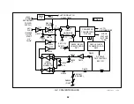
PM3394, FLUKE & PHILIPS
ch4
ch3
ch2
ch1
CH1!10.0 V~
CH2! 200mV~
CH3! 200mV~ AVG
CH4! 100 V= ALT MTB5.00us ch1+
1
2
3
4
T
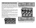
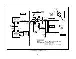
Dynamic Focus Signals
Channel
Name
Location
Voltage
1
DF Drive signal
T8002//pin 3
400Vp-p
2
Modulated power supply
T8002//pin 1
140Vp-p
3
AFC-PLS (H fly pulses)
IC5511/pin 19
10Vp-p
Time base = 5usec/div
By examining the channel 2 and 3 waveforms, the modulated power sup-
ply (ch 2) is turned off before and after the H sync pulse (ch 3). This
means there is no dynamic focus correction to the left nor right sides of
the screen. However focus correction is applied to the center of the pic-
ture as seen by the increasing voltage at the DF drive signal (ch1). The
focus correction at the center brings the focus point to the same level as
the sides.
DF Drive
The DF drive signal is manufactured in IC5511 from horizontal and verti-
cal timing pulse input at pins 19 and 21. The drive signal is output pin 11
and delayed in a chain of amps (IC5502 and Q5501). Driver transistors
Q5508-9 and Q8022-23 buffer the signal as it travels from one part of the
D board toward the other near the FBT. The final DF Output transistor
Q8018 applies the signal to T8002/pin 3.
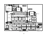
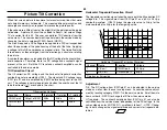
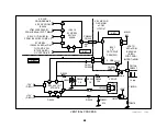
In the following waveforms you can see the low going drive signal from
IC5511/pin 11 (ch 2) become inverted and delayed (ch 3). The final drive
signal (ch 4) goes low to reduce the focus voltage at the right side of the
picture.
Modulated power supply
The modulated power supply signal is also made in IC5511 from horizon-
tal and vertical timing pulses input pins 19 and 21. IC5511’s output signal
is AC coupled to switches Q8015 and Q8016 and finally applied to T8002/
pin 1. The modulated power supply signal passes through T8002 to power
DF Output transistor Q8018 with modulated dynamic focus voltage.
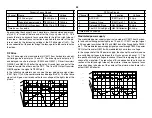
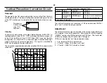
In the scope shot of the DF power supply, the channel 2 waveform shows
two switching voltages in between the H sync pulses (channel 1). The
two positive switching voltages in channel 2 result in low going B+ parts of
channel 4’s waveform. The reduction of B+ corresponds to no focus cor-
rection at the left and right sides of the picture. However, dynamic focus
correction does take place at the center of the picture when there is B+
output Q8016/Collector.
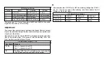
DF Drive Signals
Channel
Name
Location
Voltage
1
AFC-PLS
IC5511/pin 19
10Vp-p
2
Dynamic Drive
IC5511/pin 11
0.3Vp-p
3
Delayed DF Drive
Q8018/Base
10Vp-p
4
Final DF Drive Signal
Q8018/Collector
400Vp-p
Time Base = 5usec/div.
Summary of Contents for KV-32XBR400
Page 1: ......
Page 5: ...1 NOTES ...
Page 12: ...8 NOTES ...
Page 14: ...10 NOTES ...
Page 83: ...APPENDIX ...


