background image

000-0046140-111

Page 48 of 169 

SLG46140

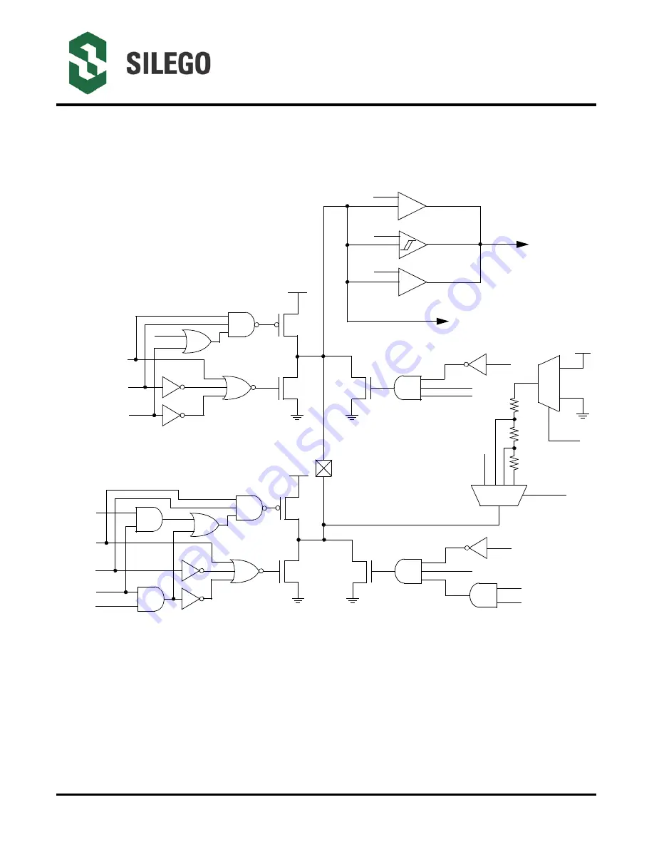
7.7   Register OE IO Structure

7.7.1   Register OE IO Structure (for Pins 6, 11) 

Figure 5. Register OE IO Structure Diagram 

PAD

Digital In

S0

S1

S2

S3

Flo

a

ting

S0

S1

pull_up_en

10 k

90 k

900 k

Res_sel[1:0]

00: floating

01: 10 k

10: 100 k

11: 1 M

wosmt_en

smt_en

lv_en

Low Voltage 

Input

Schmitt Trigger 

Input

Non-Schmitt 

Trigger Input

Mode [2:0]

000: Digital In without Schmitt Trigger, wosmt_en=1, OE = 0

001: Digital In with Schmitt Trigger, smt_en=1, OE = 0

010: Low Voltage Digital In mode, lv_en = 1, OE = 0

011: analog IO mode

100: push-pull mode, pp_en=1, OE = 1

101: NMOS open drain mode, odn_en=1, OE = 1

110: PMOS open drain mode, odp_en=1, OE = 1

111: analog IO and NMOS open-drain mode, odn_en=1 and AIO_en=1

Analog IO

Digital Out

Digital Out

OE

odn_en

OE

odn_en

2x_en

Digital Out

OE

pp_en

odp_en

Digital Out

OE

pp_en

2x_en

odp_en

Summary of Contents for GreenPAK SLG46140

Page 1: ...Operating Temperature Range 40 C to 85 C RoHS Compliant Halogen Free Pb Free 1 6 x 2 0 x 0 55 mm 0 4 mm pitch Pin Configuration Applications The extensive list of integrated components included in the SLG46140 can be used to implement these and many other functions often in combination Ambient Light Detect Battery Charge Control Fan Control Hall Effect Drive LED Control Level Shift One Shot Detect...

Page 2: ...k Up Tables LUTs Counters Delay Generators CNT0 CNT1 2 bit LUT2_0 3 bit LUT3_0 2 bit LUT2_1 2 bit LUT2_3 Combination Function Macrocells 2 bit LUT2_4 or DFF0 2 bit LUT2_5 or DFF1 3 bit LUT3_6 or Pipe Delay 3bit LUT3_5 or DFF3 3 bit LUT3_4 or DFF2 Pin 8 GND Pin 5 GPIO DFF Latches DFF4 DFF5 2 bit LUT2_2 3 bit LUT3_3 3 bit LUT3_2 3 bit LUT3_1 4 bit LUT4_1 or CNT2 4bit LUT4_0 or PGEN Digital Comparato...

Page 3: ...age Reference VREF Eight Combinatorial Lookup Tables LUTs Four 2 bit LUTs Four 3 bit LUTs Nine Combination Function Macrocells One 14 bit Delay Counter Wake Sleep Control Two Selectable DFF Latch or 2 bit LUTs Two Selectable DFF Latch or 3 bit LUTs One Selectable 16 Stage 3 Output Pipe Delay or 3 bit LUT One 8 bit Delay Counter Finite State Machine One 14 bit Delay Counter Finite State Machine One...

Page 4: ...DC Vref_IO 4 GPIO General Purpose I O or Analog Comparator 0 PGA_OUT 5 GPIO General Purpose I O or Analog Comparator 1 6 GPIO General Purpose I O or PGA 7 GPIO General Purpose I O or PGA 8 GND GND 9 GPIO General Purpose I O or ACMP1 10 GPIO General Purpose I O or ACMP0 11 GPIO General Purpose I O or AIN MUX 12 GPIO General Purpose I O 13 GPIO General Purpose I O 14 GPIO General Purpose I O ...

Page 5: ... forwarded to Silego to integrate into a production process Figure 1 Steps to create a custom Silego GreenPAK device 3URGXFW HILQLWLRQ XVWRPHU UHDWHV WKHLU RZQ GHVLJQ LQ UHHQ3 HVLJQHU 3URJUDP QJLQHHULQJ 6DPSOHV ZLWK UHHQ3 3URJUDPPHU XVWRPHU YHULILHV UHHQ3 LQ V VWHP GHVLJQ PDLO JS ILOH WR UHHQ3 VLOHJR FRP PDLO 3URGXFW GHD HILQLWLRQ UDZLQJ RU 6FKHPDWLF WR UHHQ3 VLOHJR FRP 6LOHJR SSOLFDWLRQV QJLQHHUV...

Page 6: ...000 0046140 111 Page 5 of 169 SLG46140 4 0 Ordering Information Part Number Type SLG46140V 14 pin STQFN SLG46140VTR 14 pin STQFN Tape and Reel 3k units ...

Page 7: ...e Temperature Range 65 150 C Junction Temperature 150 C ESD Protection Human Body Model 2000 V ESD Protection Charged Device Model 500 V Moisture Sensitivity Level 1 Symbol Parameter Condition Note Min Typ Max Unit VDD Supply Voltage 1 71 1 80 1 89 V IQ Quiescent Current Static Inputs and Outputs all macrocells disabled 0 08 A TA Operating Temperature 40 25 85 C VPP Programming Voltage 7 25 7 50 7...

Page 8: ...98 V VOL LOW Level Output Voltage Push Pull 1X IOL 100 A 0 010 0 020 V Push Pull 2X IOL 100 A 0 007 0 010 V Push Pull 4X IOL 100 A 0 004 0 009 V Open Drain NMOS 1X IOL 100 A 0 007 0 010 V Open Drain NMOS 2X IOL 100 A 0 002 0 010 V Open Drain NMOS 4X IOL 100 A 0 001 0 004 V IOH HIGH Level Output Pulse Current see Note 1 Push Pull 1X Open Drain PMOS 1X VOH VDD 0 2 1 053 1 690 mA Push Pull 2X Open Dr...

Page 9: ...tch Off the Chip 0 875 1 109 1 287 V RPUP Pull Up Resistance 1 M Pull Up 896 67 1075 81 1337 85 kΩ 100 k Pull Up 93 13 111 06 132 78 kΩ 10 k Pull Up 11 10 12 95 15 30 kΩ RPDWN Pull Down Resistance 1 M Pull Down 660 68 1074 06 1287 58 kΩ 100 k Pull Down 93 29 111 06 132 78 kΩ 10 k Pull Down 10 90 12 75 15 51 kΩ Note 1 DC or average current through any pin should not exceed value given in Absolute M...

Page 10: ...tage Logic Input 0 1 210 V Logic Input with Schmitt Trigger 0 0 950 V Low Level Logic Input 0 0 690 V VHYS Schmitt Trigger Hysteresis Voltage Logic Input with Schmitt Trigger 0 346 0 486 0 625 V ILKG Absolute Value ACMP Input Leakage Vin 0 V 0 42 2 49 nA Vin VDD 0 30 1 48 nA PGA Input Leakage Vin 0 V 0 05 0 21 nA Vin VDD 0 13 0 73 nA Logic Input without Schmitt Trigger Floating Leakage Vin 0 V 0 0...

Page 11: ...4 V 19 628 28 240 mA Open Drain NMOS 1X VOL 0 4 V 8 130 13 850 mA Open Drain NMOS 2X VOL 0 4 V 16 260 23 700 mA Open Drain NMOS 4X VOL 0 4 V 45 976 66 769 mA IVDD Maximum Average or DC Current Through VDD Pin Per chip side see Note 2 TJ 85 C 45 mA TJ 110 C 21 mA IGND Maximum Average or DC Current Through GND Pin Per chip side see Note 2 TJ 85 C 45 mA TJ 110 C 21 mA VO Maximal Voltage Applied to an...

Page 12: ... current through any pin should not exceed value given in Absolute Maximum Conditions Note 2 The GreenPAK s power rails are divided in two sides Pins 2 3 4 5 6 and 7 are connected to one side pins 9 10 11 12 13 and 14 to another Note 3 VDD ramp rising speed must be less than 0 6 V µs after power on Violating this specification may cause chip to restart Symbol Parameter Condition Note Min Typ Max U...

Page 13: ...tage Logic Input 0 1 840 V Logic Input with Schmitt Trigger 0 1 510 V Low Level Logic Input 0 0 780 V VHYS Schmitt Trigger Hysteresis Voltage Logic Input with Schmitt Trigger 0 443 0 618 0 792 V ILKG Absolute Value ACMP Input Leakage Vin 0 V 0 70 3 30 nA Vin VDD 0 38 1 84 nA PGA Input Leakage Vin 0 V 0 25 1 05 nA Vin VDD 0 17 0 91 nA Logic Input without Schmitt Trigger Floating Leakage Vin 0 V 0 2...

Page 14: ... 4 V 26 150 37 191 mA Open Drain NMOS 1X VOL 0 4 V 12 030 19 460 mA Open Drain NMOS 2X VOL 0 4 V 24 060 38 920 mA Open Drain NMOS 4X VOL 0 4 V 60 071 86 737 mA IVDD Maximum Average or DC Current Through VDD Pin Per chip side see Note 2 TJ 85 C 45 mA TJ 110 C 21 mA IGND Maximum Average or DC Current Through GND Pin Per chip side see Note 2 TJ 85 C 45 mA TJ 110 C 21 mA VO Maximal Voltage Applied to ...

Page 15: ... current through any pin should not exceed value given in Absolute Maximum Conditions Note 2 The GreenPAK s power rails are divided in two sides Pins 2 3 4 5 6 and 7 are connected to one side pins 9 10 11 12 13 and 14 to another Note 3 VDD ramp rising speed must be less than 0 6 V µs after power on Violating this specification may cause chip to restart Symbol Parameter Condition Note Min Typ Max U...

Page 16: ...T DLY opposite to selected edge delay 46 61 36 87 18 56 15 62 12 53 11 23 ns tpd Delay CNT DLY Shared opposite to se lected edge delay 47 30 37 16 18 78 15 78 12 68 11 77 ns tpd Delay CNT DLY Both edge detect 49 5 52 9 20 07 20 84 13 81 14 32 ns tpd Delay CNT DLY Rising edge detect 52 39 21 32 14 67 ns tpd Delay CNT DLY Falling edge detect 55 94 22 15 15 27 ns tw Width CNT DLY Both edge detect 25 ...

Page 17: ...elay PDLY 3Cells Falling edge detect 35 60 13 65 9 37 ns tpd Delay PDLY 4Cells Both edge detect 30 76 35 23 12 03 13 53 8 42 9 25 ns tpd Delay PDLY 4Cells delayed output Both edge detect 684 15 688 20 267 31 268 47 168 33 169 41 ns tpd Delay PDLY4Cells delayed output Rising edge detect 685 08 267 57 168 46 ns tpd Delay PDLY 4Cells delayed output Fall ing edge detect 688 67 268 47 169 54 ns tpd Del...

Page 18: ...tw Width PDLY 4Cells Both edge detect 1383 47 1385 73 611 73 612 67 445 93 446 80 ns tw Width PDLY 4Cells delayed output Both edge detect 1371 27 1373 67 600 93 602 07 439 00 439 93 ns tw Width PDLY4Cells delayed output Rising edge detect 1371 47 601 13 438 73 ns tw Width PDLY 4Cells delayed output Fall ing edge detect 1373 80 602 20 439 73 ns tw Width PDLY 4Cells Rising edge detect 1383 40 611 67...

Page 19: ...t Schmitt trigger Push Pull Z to 0 36 09 13 83 9 51 ns tpd Delay Digital Input without Schmitt Trig ger Push Pull 1x 40 92 35 45 15 32 14 79 10 60 10 52 ns tpd Delay Digital Input without Schmitt Trig ger Push Pull 2x 39 61 34 98 14 8 14 37 10 31 10 17 ns tpd Delay Digital Input without Schmitt Trig ger Push Pull 4x 37 84 33 40 14 11 13 80 9 93 9 92 ns Symbol Parameter Note VDD 1 8V VDD 3 3V VDD 5...

Page 20: ...le end mode Gain 1x 69 44 73 44 77 36 uA PGA Single end mode Gain 2x 116 42 91 50 111 10 uA PGA Single end mode Gain 4x 117 87 97 20 114 72 uA DAC0 Power on 48 24 40 40 44 47 uA DAC1 DCMP1 Input 62 83 55 04 59 11 uA ADC Single end mode Vref 1 2 V Force analog part Enable Speed selection 100 kHz RC OSC 25 kHz First Clock predivider by 1 Sample rate 1 56 kHz 172 24 166 10 171 01 uA ADC Single end mo...

Page 21: ...5 V 10 24 739 25 428 23 976 25 714 23 689 26 550 2 5 V 4 5 V 24 842 25 147 23 937 25 691 23 803 26 642 1 71 V 5 5 V 24 380 25 701 23 891 25 989 23 429 27 036 Table 4 25 kHz RC OSC frequency error error calculated relative to nominal value Power Supply Range VDD V Temperature Range 25 C 0 C 85 C 40 C 85 C Error at Minimum Error at Maximum Error at Minimum Error at Maximum Error at Minimum Error at ...

Page 22: ... 2 173 1 905 2 200 1 802 2 200 2 5 V 4 5 V 1 924 2 069 1 884 2 106 1 783 2 106 1 71 V 5 5 V 1 832 2 180 1 782 2 191 1 782 2 209 Table 6 2 MHz RC OSC frequency error error calculated relative to nominal value Power Supply Range VDD V Temperature Range 25 C 0 C 85 C 40 C 85 C Error at Minimum Error at Maximum Error at Minimum Error at Maximum Error at Minimum Error at Maximum 1 8 V 5 2 36 1 38 5 29 ...

Page 23: ...2 992 28 176 22 224 28 176 2 5 V 4 5 V 23 617 28 095 23 299 28 095 22 528 28 095 1 71 V 5 5 V 22 482 28 167 21 855 28 176 21 855 28 176 Table 8 25 MHz Ring OSC Frequency Error Error Calculated Relative to Nominal Value Power Supply Range VDD V Temperature Range 25 C 0 C 85 C 40 C 85 C Error at Minimum Error at Maximum Error at Minimum Error at Maximum Error at Minimum Error at Maximum 1 8 V 5 11 8...

Page 24: ... 10 15 69 19 84 16 33 20 27 19 75 20 57 2 5 V 4 5 V 15 74 18 82 16 43 19 25 19 88 20 03 1 71 V 5 5 V 15 74 19 84 16 43 20 27 19 88 20 57 Table 11 Oscillators Power On Delay at Room Temperature RC OSC Power Setting Auto Power On RC OSC Clock to Matrix Input Enable Power Supply Range VDD V LF OSC RC OSC 2 MHz RC OSC 25 kHz RING OSC Typical Value µs Maximum Value µs Typical Value ns Maximum Value ns ...

Page 25: ... Offset Voltage Low Bandwidth Enable Vhys 0 mV Gain 1 Vref 50 1200 mV VDD 1 71 5 5 V T 25 C 10 2 9 0 mV T 40 85 C 15 3 13 4 mV Low Bandwidth Disable Vhys 0 mV Gain 1 Vref 50 1200 mV VDD 1 71 5 5 V T 25 C 6 8 6 3 mV T 40 85 C 7 2 6 6 mV tstart ACMP Start Time ACMP Power On delay Minimal required wake time for the Wake and Sleep function Regulator and Charge Pump set to automatic ON OFF BG 550 μs T ...

Page 26: ...44 4 mV VHYS 50 mV VIL Vin VHYS VIH VHYS LB Enabled T 40 85 C 35 1 72 4 mV LB Disabled T 40 85 C 43 8 55 6 mV VHYS 200 mV VIL Vin VHYS VIH VHYS LB Enabled T 40 85 C 184 8 224 2 mV LB Disabled T 40 85 C 189 7 207 9 mV Rsin Series Input Resistance Gain 1x 100 0 Gain 0 5x 1 0 Gain 0 33x 0 8 Gain 0 25x 1 0 PROP Propagation Delay Response Time Low Bandwidth Enable Gain 1 VDD 1 71 5 5 V Overdrive 5 mV L...

Page 27: ...mV 0 70 0 79 G 0 33 VDD 1 71V Vref 50 1200 mV 0 58 0 95 G 0 33 VDD 3 3 V Vref 50 1200 mV 0 70 0 82 G 0 33 VDD 5 5 V Vref 50 1200 mV 0 54 0 88 G 0 25 VDD 1 71V Vref 50 1200 mV 0 49 1 21 G 0 25 VDD 3 3 V Vref 50 1200 mV 0 65 1 00 G 0 25 VDD 5 5 V Vref 50 1200 mV 0 41 1 18 Vref Internal Vref error Vref 1200 mV VDD 1 8 V 5 T 25 C 0 96 0 95 T 40 85 C 1 30 1 12 VDD 3 3 V 10 T 25 C 1 02 1 03 T 40 85 C 1 ...

Page 28: ... 2060 mV G 1 30 1030 mV G 2 20 520 mV G 4 15 265 mV G 8 12 137 mV ZE Offset Zero Error G 0 25 T 25 C VDD 5V 10 1 7 LSB G 0 5 T 25 C VDD 2 5 to 5 5 V 2 6 LSB G 1 T 25 C 3 LSB G 2 2 6 LSB G 4 3 3 LSB G 8 4 6 LSB dZE dT Offset Zero Error Temperature Drift G 0 25 VDD 5V 10 0 008 C G 0 5 VDD 2 5 to 5 5 V 0 009 C G 1 0 01 C G 2 0 014 C G 4 0 025 C G 8 0 048 C GE Gain Error G 0 25 T 25 C VDD 5V 10 1 5 LS...

Page 29: ... 10 3 2 LSB G 0 5 T 25 C VDD 2 5 to 5 5 V 1 9 LSB VDD 2 5 to 5 5 V 3 4 LSB G 1 T 25 C 1 7 LSB 3 2 LSB G 2 T 25 C 1 8 LSB 2 9 LSB G 4 T 25 C 1 8 LSB 2 7 LSB G 8 T 25 C 1 6 LSB 2 6 LSB DNL Differential Non Linearity G 0 25 0 5 1 2 4 8 0 5 LSB NOISE 0 5 LSB Table 13 Single Ended ADC Operation T 40 to 85 C VDD 1 71 to 5 5 V unless otherwise specified Symbol Parameter Description Note Conditions Min Ma...

Page 30: ... 8 V 5 400 550 mV VDD 3 3 V 10 400 950 mV VDD 5 V 10 400 950 mV ZE Offset Zero Error G 1 T 25 C 2 5 LSB G 2 2 7 LSB G 4 3 3 LSB G 8 4 6 LSB G 16 6 8 LSB dZE dT Offset Zero Error Temperature Drift G 1 0 014 C G 2 0 015 C G 4 0 02 C G 8 0 032 C G 16 0 1 C GE Gain Error G 1 T 25 C 0 8 LSB G 2 0 8 LSB G 4 0 5 LSB G 8 1 LSB G 16 1 LSB dGE dT Gain Error Temperature Drift G 1 0 007 C G 2 0 007 C G 4 0 00...

Page 31: ...ange is given for stable CMRR 34 dB Note 2 To ensure linear operation absolute input voltage on each pin should not exceed VDD 0 5 DNL Differential Non Linearity G 1 2 4 8 16 0 5 LSB NOISE 0 5 LSB Symbol Parameter Description Note Conditions Min Max Unit ...

Page 32: ...Vinn Negative input voltage range G 1 2 4 VDD 1 8 V 5 500 500 mV VDD 3 3 V 10 500 1250 mV VDD 5 V 10 500 1250 mV ZE Offset Zero Error G 1 T 25 C VDD 2 0 to 5 5 V 2 6 LSB G 2 T 25 C 2 7 LSB G 4 3 3 LSB dZE dT Offset Zero Error Temperature Drift G 1 T 25 C VDD 2 0 to 5 5 V 0 012 C G 2 T 25 C 0 013 C G 4 0 018 C GE Gain Error G 1 T 25 C VDD 2 0 to 5 5 V 1 9 LSB G 2 T 25 C 2 4 LSB G 4 1 4 LSB dGE dT G...

Page 33: ... 2 12 1 mV G 2 T 25 C 3 4 13 7 mV G 4 T 25 C 3 2 12 0 mV G 8 T 25 C 3 2 11 6 mV dVos dT Vos RTI Temperature Drift G 0 25 VDD 5V 10 0 0097 0 0584 mV C G 0 5 VDD 2 5 to 5 5 V 0 0058 0 0345 mV C G 1 0 0018 0 0111 mV C G 2 0 0031 0 0186 mV C G 4 0 0028 0 0167 mV C G 8 0 0026 0 0158 mV C ΔG Gain Error G 0 25 VDD 5V 10 0 822 0 562 1 945 G 0 5 VDD 2 5 to 5 5 V 0 877 0 196 1 260 G 1 0 118 0 012 0 093 G 2 ...

Page 34: ...ature Drift G 1 0 0124 0 0551 mV C G 2 0 0118 0 0658 mV C G 4 0 0148 0 0884 mV C G 8 0 0240 0 1416 mV C G 16 0 0432 0 256 mV C ΔG Gain Error G 1 1 080 0 194 0 664 G 2 1 761 0 568 0 629 G 4 2 573 0 929 0 656 G 8 3 553 1 620 0 225 G 16 3 720 1 808 0 106 Vind lin Linear Differential Input Voltage Range G 1 452 578 mV G 2 229 289 mV G 4 115 145 mV G 8 57 72 mV G 16 29 32 mV CMRR Common Mode Rejection ...

Page 35: ... 25 C 1 5 5 5 mV G 4 T 25 C 2 1 6 4 mV dVos dT Vos RTO Temperature Drift G 1 0 0088 0 0493 mV C G 2 0 0098 0 0588 mV C G 4 0 0128 0 0772 mV C ΔG Gain Error G 1 0 916 0 455 0 549 G 2 1 855 0 567 0 685 G 4 2 559 0 918 0 735 Vind lin Linear Differential Input Voltage Range G 1 0 834 mV G 2 0 394 mV G 4 0 239 mV CMRR Common Mode Rejection Rate G 1 32 dB G 2 38 dB G 4 44 dB Vinn Negative Input Voltage ...

Page 36: ...pecified Symbol Parameter Description Note Conditions Min Typ Max Unit Vos Offset Voltage RTI see Note 1 All gains T 25 C VDD 3 3 V 1 9 11 2 mV ΔG Gain Error G 1 1 080 0 194 0 664 G 2 1 761 0 568 0 629 G 4 2 573 0 929 0 656 G 8 3 553 1 620 0 225 G 16 3 720 1 808 0 106 CMRR Common Mode Rejection Rate G 1 32 dB G 2 38 dB G 4 44 dB G 8 50 dB G 16 56 dB Vinn Negative Input Voltage Range All gains VDD ...

Page 37: ...e 1 2 4X in Pseudo Differential mode and 0 25 0 5 1 2 4 8x in single ended mode SPI output format 6 4 Digital to Analog Converter Two 8 bit Digital to Analog Converters 0 to 1 V 6 5 Analog Comparators 2 total Selectable hysteresis 0 mV 25 mV 50 mV 200 mV Internal or external Vref Selectable gain 1x 0 5x 0 33x 0 25x Low bandwidth 6 6 Voltage Reference Used for references on Analog Comparators Can a...

Page 38: ...illator 25 kHz and 2 MHz selectable frequency Pre divider 4 OSC 1 OSC 2 OSC 4 and OSC 8 Output to Matrix OSC 1 OSC 2 OSC 3 OSC 4 OSC 8 OSC 12 OSC 24 OSC 64 Output to CNT DLY FSM PWM_ramp OSC 1 OSC 4 OSC 12 OSC 24 OSC 64 Output to ADC OSC 1 OSC 16 6 12 Low Frequency LF Oscillator 1 9 kHz OSC 1 OSC 2 OSC 4 OSC 16 dividers 6 13 Ring Oscillator 25 MHz Post divider OSC 1 OSC 4 OSC 8 OSC 16 Output to Ma...

Page 39: ...elect Pin 12 GPIO with OE Pin 13 GPIO with OE Pin 14 GPIO with OE Programming Mode pin definitions are as follows Pin 1 VDD Power Supply Pin 2 VPP Programming Voltage Pin 3 RTSB Pin 10 Programming Mode Control Pin 11 Programming ID Pin 12 Programming SDIO Pin 13 Programming SRDWB Pin 14 Programming SCL 7 1 Input Modes Digital Input Each GPI GPIO pin can be configured as a Digital input with withou...

Page 40: ...ltage digital input 11 Reserved PIN 2 Pull Down Resistor Value Selection reg 764 763 00 Floating 01 10 k Resistor 10 100 k Resistor 11 1 M Resistor PIN 2 Pull Up Down Resistor Selection reg 765 0 Pull Down Resistor 1 Pull Up Resistor Table 21 PIN 3 Register Settings Signal Function Register Bit Address Register Definition PIN 3 Input Mode Control reg 767 766 00 Digital Input without Schmitt trigge...

Page 41: ...7 00 Floating 01 10 k Resistor 10 100 k Resistor 11 1 M Resistor PIN 4 Pull Up Down Resistor Selection reg 779 0 Pull Down Resistor 1 Pull Up Resistor Table 23 PIN 5 Register Settings Signal Function Register Bit Address Register Definition PIN 5 Input Mode Control reg 781 780 00 Digital Input without Schmitt trigger 01 Digital Input with Schmitt trigger 10 Low Voltage Digital Input 11 Analog Inpu...

Page 42: ...stor 11 1 M Resistor PIN 6 Pull Up Down Resistor Selection reg 793 0 Pull Down Resistor 1 Pull Up Resistor PIN 6 Output Driver Current x2 Enable reg 794 0 Disable 1 Enable Table 25 PIN 7 Register Settings Signal Function Register Bit Address Register Definition PIN 7 Input Mode Control reg 796 795 00 Digital Input without Schmitt trigger 01 Digital Input with Schmitt trigger 10 Low Voltage Digital...

Page 43: ...ull Up Down Resistor Selection reg 808 0 Pull Down Resistor 1 Pull Up Resistor PIN 9 4x Driver Enable reg 809 0 Disable 1 Enable Table 27 PIN 10 Register Settings Signal Function Register Bit Address Register Definition PIN 10 Input Mode Control reg 813 811 000 Digital in without Schmitt Trigger 001 Digital in with Schmitt Trigger 010 Low Voltage Digital In 011 Analog IO 100 Push Pull Mode 101 NMO...

Page 44: ...stor 11 1 M Resistor PIN 11 Pull Up Down Resistor Selection reg 825 0 Pull Down Resistor 1 Pull Up Resistor PIN 11 Output Driver Current x2 Enable reg 826 0 Disable 1 Enable Table 29 PIN 12 Register Settings Signal Function Register Bit Address Register Definition PIN 12 Input Mode Control reg 828 827 00 Digital Input without Schmitt trigger 01 Digital Input with Schmitt trigger 10 Low Voltage Dig...

Page 45: ...38 00 Floating 01 10 k Resistor 10 100 k Resistor 11 1 M Resistor PIN 13 Pull Up Down Resistor Selection reg 840 0 Pull Down Resistor 1 Pull Up Resistor Table 31 PIN 14 Register Settings Signal Function Register Bit Address Register Definition PIN 14 Input Mode Control reg 842 841 00 Digital Input without Schmitt trigger 01 Digital Input with Schmitt trigger 10 Low Voltage Digital Input 11 Analog ...

Page 46: ...loating 10 k 90 k 900 k Res_sel 1 0 00 floating 01 10 k 10 100 k 11 1 M wo_smt_en wi_smt_en lv_en Low Voltage Input SchmittTrigger Input Non Schmitt Trigger Input Input Mode 1 0 00 Digital In without Schmitt Trigger wosmt_en 1 01 Digital In with Schmitt Trigger smt_en 1 10 Low Voltage Digital In mode lv_en 1 11 Reserved S0 S1 pull_up_en ...

Page 47: ...e Input SchmittTrigger Input Non Schmitt Trigger Input Input Mode 1 0 00 Digital In without Schmitt Trigger wosmt_en 1 01 Digital In with Schmitt Trigger smt_en 1 10 Low Voltage Digital In mode lv_en 1 11 Analog IO mode Output Mode 1 0 00 1x push pull mode pp1x_en 1 01 2x push pull mode pp2x_en 1 pp1x_en 1 10 1x NMOS open drain mode od1x_en 1 11 2x NMOS open drain mode od2x_en 1 od1x_en 1 Analog I...

Page 48: ...x OE IO structures see above section Figure 4 Matrix OE IO 4x Drive Structure Diagram PAD PIN 9 Input Mode 1 0 Output Mode 1 0 Pull up Enable Res_Sel 1 0 OE Dout Matrix OE GPIO PAD PAD Input Mode 1 0 Output Mode 1 0 Pull up Enable Res_Sel 1 0 OE Dout Matrix OE GPIO PAD PAD GND GND Mode 1 0 Mode 3 2 Pull up Enable Res_Sel 1 0 OE Dout 4x_en ...

Page 49: ...chmittTrigger Input Non Schmitt Trigger Input Mode 2 0 000 Digital In without Schmitt Trigger wosmt_en 1 OE 0 001 Digital In with Schmitt Trigger smt_en 1 OE 0 010 Low Voltage Digital In mode lv_en 1 OE 0 011 analog IO mode 100 push pull mode pp_en 1 OE 1 101 NMOS open drain mode odn_en 1 OE 1 110 PMOS open drain mode odp_en 1 OE 1 111 analog IO and NMOS open drain mode odn_en 1 and AIO_en 1 Analo...

Page 50: ... above section Figure 6 Register OE IO 4x Drive Structure Diagram PAD PIN 10 Mode 2 0 2x_en Pull up Enable Res_Sel 1 0 Dout Register OE GPIO PAD PAD GND GND Mode 2 0 Mode 3 2 Pull up Enable Res_Sel 1 0 Dout Mode 2 0 2x_en Pull up Enable Res_Sel 1 0 Dout Register OE GPIO PAD PAD 4x_en S0 S1 Mode_4x 2 0 S1 S0 Mode 2 Mode 1 0 4x_en 4x_en Mode_4x 2 Mode_4x 1 0 Mode_4x 2 0 ...

Page 51: ...Matrix has 64 inputs and 81 outputs Each of the 64 inputs to the Connection Matrix is hard wired to a particular source macrocell including I O pins LUTs analog comparators other resources and VDD The input to a digital macrocell uses a 6 bit register to select one of these 64 input lines For a complete list of the SLG46140 s register table see Section 23 0 Appendix A SLG46140 Register Definition ...

Page 52: ...b or setb 0 0 1 1 1 0 15 DFF4 Latch4 QB output with resetb or setb 0 0 1 1 1 1 16 DFF5 Latch5 Q output with resetb or setb 0 1 0 0 0 0 17 DFF5 Latch5 QB output with resetb or setb 0 1 0 0 0 1 18 1 PIPE OUT of pipe delay LUT3_6 output 0 1 0 0 1 0 19 OUT0 of pipe delay 0 1 0 0 1 1 20 OUT1 of pipe delay 0 1 0 1 0 0 21 edgedet progdly output 0 1 0 1 0 1 22 PIN2 output 0 1 0 1 1 0 23 PIN3 output 0 1 0 ...

Page 53: ...negative 1 0 1 1 1 0 47 SPI interrupt 1 0 1 1 1 1 48 ACMP0 output 1 1 0 0 0 0 49 ACMP1 output 1 1 0 0 0 1 50 ADC interrupt 1 1 0 0 1 0 51 bg_ok signal delay 200ns 1 1 0 0 1 1 52 power detector output 1 1 0 1 0 0 53 no divider RC oscillator output 1 1 0 1 0 1 54 GROUND 1 1 0 1 1 0 55 GROUND 1 1 0 1 1 1 56 GROUND 1 1 1 0 0 0 57 GROUND 1 1 1 0 0 1 58 GROUND 1 1 1 0 1 0 59 GROUND 1 1 1 0 1 1 60 GROUND...

Page 54: ...14 reg 95 90 In0 of LUT3_1 15 reg 101 96 In1 of LUT3_1 16 reg 107 102 In2 of LUT3_1 17 reg 113 108 In0 of LUT3_2 18 reg 119 114 In1 of LUT3_2 19 reg 125 120 In2 of LUT3_2 20 reg 131 126 In0 of LUT3_3 21 reg 137 132 In1 of LUT3_3 22 reg 143 138 In2 of LUT3_3 23 reg 149 144 In0 of LUT3_4 Resetb of DFF Latch 2 24 reg 155 150 In1 of LUT3_4 Data of DFF Latch 2 25 reg 161 156 In2 of LUT3_4 Clock of DFF ...

Page 55: ...5 330 Digital Output of PIN10 55 reg 341 336 Digital Output of PIN11 56 reg 347 342 Digital Output of PIN12 57 reg 353 348 OE of PIN12 58 reg 359 354 Digital Output of PIN13 59 reg 365 360 OE of PIN13 60 reg 371 366 Digital Output of PIN14 61 reg 377 372 OE of PIN14 62 reg 383 378 ADC Power Down 1 Power Down 63 reg 389 384 PDB Power Down for ACMP0 0 Power Down 64 reg 395 390 PDB Power Down for ACM...

Page 56: ... Positive Input and PWM DCMP1 Negative Input Register Selection Bit 0 76 reg 467 462 PWM DCMP0 Positive Input and PWM DCMP1 Negative Input Register Selection Bit 1 77 reg 473 468 PWM Power Down 1 Power Down 78 reg 479 474 CSB of SPI 79 reg 485 480 SCLK of SPI 80 Table 33 Matrix Output Table Register Bit Address Matrix Output Signal Function Matrix Output Number ...

Page 57: ...n ADC is disabled Please see section 9 3 2 PGA Output for more details User controlled inputs and outputs of the ADC are listed below Inputs CH SELECTOR Single Ended Mode ADC Selection and Analog Input Mux Control Signal PIN 11 VDD IN Single Ended Mode Input PIN6 or PIN7 and Differential Mode Positive Input PIN6 IN Differential Mode Negative Input PIN 7 or DAC0 VREF ADC Voltage Reference Input ADC...

Page 58: ...34 532 PGA OUT ADC Programmable Gain Amplifier PAR DATA INT OUT CLK VREF reg 546 545 VDD 0 25 Reserved ADC VREF Wake Sleep En reg 557 DAC_in_en reg 529 reg 578 reg 530 0 1 DAC 0 0 1 8 bit reg 555 548 DCMP1_IN reg 547 SER DATA PGAOUT_en reg 559 16 ADC CLK SRC reg 580 579 00 01 10 11 Diff_mode_en reg 531 pseudo_en reg 536 Wake Sleep Signal Ring Osc Ext CLK2 matrix1_out67 RC Osc SPI CLK to ACMP ...

Page 59: ...6x Pseudo Differential 1x 2x 4x PGA inputs CH SELECTOR Single Ended Mode ADC Selection and Analog Input Mux Control Signal PIN 11 VDD IN Single Ended Mode Input PIN6 or PIN7 and Differential Mode Positive Input PIN6 IN Differential Mode Negative Input PIN7 or DAC0 PGA output is connected directly to ADC input Also it is possible to connect PIN7 to PGA output reg 886 when ADC is not in use only The...

Page 60: ...l Pseudo Differential mode with ADC in POWER DOWN state are given in specifications section for information only Note 1 PGA operation in Differential Pseudo Differential mode with ADC in POWER DOWN state is not recommended to use Note 2 Toggling ADC POWER DOWN mode will also toggle the PGA output reference macrocell that will influence the ACMP input voltage PGA has a few output connection possibi...

Page 61: ...ifferential operation 110 16x For differential operation only 111 Reserved PGA power on signal 535 0 power down 1 power on Note in ADC wake sleep dynamic on off mode must be set to 0 PGA Pseudo Differential Mode Enable 536 0 Disable 1 Enable DAC0 Input Selection 547 0 From register 1 From DCMP1 s input DAC0 8 Bit Register Control 855 548 00 DAC0 output Is 0 FF DAC0 s output Is 1 V Force ADC Analog...

Page 62: ...5 30 17 1 15 1 13 1 11 0 9 0 7 0 4 9 2 9 0 9 1 1 3 2 5 2 7 2 9 3 11 3 13 3 15 3 21 4 Percentage of Occurrences Vos mV 200 samples VDD 3 3 V T 25 C Figure 13 PGA Input Offset Distribution Single Ended Mode G 1 0 5 10 15 20 25 30 8 6 7 6 6 6 5 6 4 5 3 5 2 5 1 5 0 4 0 6 1 6 2 6 3 7 4 7 5 7 6 7 7 8 10 8 Percentage of Occurrences Vos mV 200 samples VDD 3 3 V T 25 C Figure 14 PGA Input Offset Distributi...

Page 63: ...Distribution Single Ended Mode G 8 0 2 4 6 8 10 12 14 16 18 20 5 4 4 9 4 3 3 8 3 2 2 7 2 1 1 6 1 0 0 4 0 1 0 7 1 2 1 8 2 3 2 9 3 4 5 1 Percentage of Occurrences Vos mV 200 samples VDD 3 3 V T 25 C Figure 17 Typical PGA Gain Error vs Vin Single Ended Mode G 1 VDD 1 71 V 2 1 5 1 0 5 0 0 5 0 200 400 600 800 1000 1200 Gain Error Vin 40 C 25 C 85 C Figure 18 Typical PGA Gain Error vs Vin Single Ended M...

Page 64: ...ode G 8 VDD 5 5 V 5 4 5 4 3 5 3 2 5 2 1 5 1 0 5 0 0 20 40 60 80 100 120 140 160 Gain Error Vin 40 C 25 C 85 C Figure 21 PGA Input Vind Range Multiplied by Gain vs Vcm Differential Mode 600 400 200 0 200 400 600 0 500 1000 1500 2000 2500 3000 Vin range G mV Vcm mV Vdd 1 71V Vdd 3 3 V Vdd 5 5 V Figure 22 Typical PGA Gain Error vs Vin Differential Mode G 1 VDD 1 71 V 2 1 8 1 6 1 4 1 2 1 0 8 0 6 0 4 0...

Page 65: ...ferential Mode G 16 VDD 1 71 V 3 2 5 2 1 5 1 0 5 0 40 30 20 10 0 10 20 30 40 Gain Error Vin 40 C 25 C 85 C Figure 25 Typical PGA Gain Error vs Vin Differential Mode G 16 VDD 5 5 V 3 2 5 2 1 5 1 0 5 0 40 30 20 10 0 10 20 30 40 Gain Error Vin 40 C 25 C 85 C Figure 26 PGA Input Vind Range Multiplied by Gain vs Vinn Pseudo Differential Mode G 1 0 200 400 600 800 1000 1200 0 200 400 600 800 1000 1200 1...

Page 66: ... Vinn Pseudo Differential Mode G 4 0 200 400 600 800 1000 1200 0 200 400 600 800 1000 1200 1400 1600 Vin range mV Vinn mV Vdd 3 3V Vdd 1 71 Figure 29 Typical PGA Gain Error vs Vin Pseudo Differential Mode G 1 VDD 2 0 V 2 1 8 1 6 1 4 1 2 1 0 8 0 6 0 4 0 2 0 0 200 400 600 800 1000 1200 Gain Error Vin 40 C 25 C 85 C Figure 30 Typical PGA Gain Error vs Vin Pseudo Differential Mode G 1 VDD 5 5 V 2 1 8 ...

Page 67: ...s one half of the reference voltage VOUT PGA VIN ADC G Vinp Vos RTI for SE mode VOUT PGA VIN ADC G Vind Vos RTO for DI and PD mode Vos PGA offset voltage RTI and RTO denotes referred to input and referred to output Vos G PGA nominal gain Vind PGA input voltage differential Vind Vinp Vinn Figure 31 Typical PGA Gain Error vs Vin Pseudo Differential Mode G 4 VDD 1 71 V 3 2 5 2 1 5 1 0 5 0 0 50 100 15...

Page 68: ... ended mode Vind Vinp Vinp min and Vinp max positive input voltage for bit0 and bit255 correspondingly can be found in ADC specifications Differential and Pseudo Differential mode Vind min and Vind max differential input voltage for bit0 and bit255 correspondingly can be found in ADC specifications Least significant bit size LSB calculates as follows where FS is full scale range FS Vind max Vind m...

Page 69: ...lled by connection matrix output 63 and the analog macrocell will remain on With this feature the first ADC power on with the rest of the analog macrocell will be approximately 500 s the next power cycle the ADC power on ADC only time is 5 s 9 7 ADC Clock Source The ADC clock source comes from either the internal RC Oscillator Matrix1_Out73 Ring Oscillator or SPI CLK The ADC requires 16 clock cycl...

Page 70: ...e 8 Bit Serial Data This PD signal needs to be held for at least 16 ADC_CLK cycles The ADC_CLK is determined by either the RC Osc Ring Osc Matrix_Out67 or SPI CLK 9 8 2 ADC Parallel Output The 16 bit parallel data can be output from the ADC logic cell to either the DCMP PWM or FSM logic cells within the SLG46140 device To initialize the PAR DATA the ADC needs a Power Down signal which can be confi...

Page 71: ...rrupt Output Timing Diagram Power_Down CLK case 1 D7 D0 T_ADC_startup 500 s force analog disable 1 3 5 2 4 6 7 8 9 11 13 10 12 14 15 16 SER DATA PAR DATA SER DATA PAR DATA ADC_int CLK case 2 1 3 5 2 4 6 7 8 9 11 13 10 12 14 15 16 1 1 16 16 Bandgap OK First pulse T_ADC_startup 5 s force analog enable ...

Page 72: ...refer to Table 34 Table 35 ADC Register Settings Signal Function Register Bit Address Register Definition ADC Speed Selection 543 542 00 Reserved 01 Reserved 10 100 kHz 11 Reserved ADC Vref Source Select 546 545 00 ADC VREF 01 Reserved 10 1 4 Vdd 11 None ADC Wake Sleep Enable 557 0 Disable 1 Enable ...

Page 73: ...FSM1 7 0 DAC0 Outputs PIN3 PGA negative input 00 0 V FF 1 V ACMP0 negative input ACMP1 negative input DAC1 Inputs Registers 8LSBs SPI FSM0 7 0 FSM1 7 0 DAC1 Outputs ACMP0 negative input ACMP1 negative input If a DAC0 output is connected to external Pin3 of SLG46140 s it is necessary to enable this external pin as analog input output reg 544 0 DAC0 power off 1 DAC0 power on reg 538 0 DAC1 power off...

Page 74: ...agram Figure 37 DAC1 Functional Diagram Register DCMP1 s neg input DAC0 Pin3_aio_en reg 767 766 11 Vref Out_1 Pin3 PGA negative input ACMP0 negative input ACMP1 negative input reg 528 527 01 10 11 reg 547 0 1 reg 544 PWR DOWN ACMP1 negative input ACMP0 negative input Register DCMP1 s neg input DAC1 reg 556 1 0 reg 538 PWR DOWN ...

Page 75: ...reg 538 DAC1 power on signal 0 power down 1 power on reg 544 DAC0 power on signal 0 power down 1 power on When DAC0 used only need set this bit reg 547 DAC0 input selection 0 from register 1 from DCMP1 s input reg 555 548 DAC0 8 bit register control 00 DAC0 output is 0 FF DAC0 s output is 1 V reg 556 DAC1 input selection 0 from DCMP1 s Negative input 1 from register reg 558 Force ADC analog part o...

Page 76: ...single output which goes back into the connection matrix Figure 38 2 bit LUTs 2 bit LUT0 OUT IN1 IN0 reg 851 848 From Connection Matrix Output 0 From Connection Matrix Output 1 To Connection Matrix Input 1 2 bit LUT1 OUT IN1 IN0 reg 855 852 From Connection Matrix Output 2 From Connection Matrix Output 3 To Connection Matrix Input 2 2 bit LUT2 OUT IN1 IN0 reg 859 856 From Connection Matrix Output 4...

Page 77: ...ction Matrix Output 12 From Connection Matrix Output 13 To Connection Matrix Input 7 3 bit LUT1 OUT IN1 IN0 reg 889 882 From Connection Matrix Output 15 From Connection Matrix Output 16 To Connection Matrix Input 8 IN2 From Connection Matrix Output 14 IN2 From Connection Matrix Output 17 3 bit LUT2 OUT IN1 IN0 reg 897 890 From Connection Matrix Output 18 From Connection Matrix Output 19 To Connect...

Page 78: ...77 1 0 0 reg 878 1 0 1 reg 879 1 1 0 reg 880 1 1 1 reg 881 Table 43 3 bit LUT1 Truth Table IN2 IN1 IN0 OUT 0 0 0 reg 882 0 0 1 reg 883 0 1 0 reg 884 0 1 1 reg 885 1 0 0 reg 886 1 0 1 reg 887 1 1 0 reg 888 1 1 1 reg 889 Table 44 3 bit LUT2 Truth Table IN2 IN1 IN0 OUT 0 0 0 reg 890 0 0 1 reg 891 0 1 0 reg 892 0 1 1 reg 893 1 0 0 reg 894 1 0 1 reg 895 1 1 0 reg 896 1 1 1 reg 897 Table 45 3 bit LUT3 T...

Page 79: ... including the following standard digital logic devices AND NAND OR NOR XOR XNOR When used as a D Flip Flop Latch the source and destination of the inputs and outputs for the DFF Latches are configured from the connection matrix All DFF Latch macrocells have user selection for initial state and all have the option to connect both the Q and Q Bar outputs to the connection matrix The macrocells DFF2...

Page 80: ...67 864 reg 868 From Connection Matrix Output 8 Q nQ reg 865 Output Select Q or nQ 0 1 0 1 0 1 reg 864 Latch Mode Select reg 866 Init Polarity Select DFF1 CLK D 2 bit LUT5 OUT IN0 IN1 To Connection Matrix Input 6 4 bits NVM From Connection Matrix Output 11 1 bit NVM reg 872 869 reg 873 From Connection Matrix Output 10 Q nQ reg 870 Output Select Q or nQ 0 1 0 1 0 1 reg 869 Latch Mode Select reg 871 ...

Page 81: ... 1 nQ output DFF0 Initial Polarity Select 866 0 Low 1 High LUT2_4 or DFF0 Select 868 0 LUT2_4 1 DFF0 Table 50 LUT2_5 or DFF1 Register Settings Signal Function Register Bit Address Register Definition DFF1 or Latch Select 869 0 DFF function 1 Latch function DFF1 Output Select 870 0 Q output 1 nQ output DFF1 Initial Polarity Select 871 0 Low 1 High LUT2_5 or DFF1 Select 873 0 LUT2_5 1 DFF1 Table 47 ...

Page 82: ...Flop with the output going back to the connection matrix Figure 42 3 bit LUT4 or DFF2 Figure 43 3 bit LUT5 or DFF3 DFF2 CLK D To Connection Matrix Input 11 8 bits NVM From Connection Matrix Output 26 1 bit NVM 3 bit LUT4 OUT IN1 IN2 IN0 nRST nSET From Connection Matrix Output 25 From Connection Matrix Output 24 reg 913 906 reg 914 reg 907 Output Select Q or nQ Q nQ reg 906 Latch Mode Select reg 90...

Page 83: ...ut 0 nRST from matrix out DFF2 Initial Polarity Select reg 909 0 Low 1 High LUT3_4 or DFF2 Select reg 914 0 LUT3_4 1 DFF2 Table 54 DFF3 Register Settings Signal Function Register Bit Address Register Definition DFF3 or Latch Select reg 915 0 DFF function 1 Latch function DFF3 Output Select reg 916 0 Q output 1 nQ output DFF3 nRST nSET Select reg 917 1 nSET from matrix out 0 nRST from matrix out DF...

Page 84: ...ions for 1 16 stages of delay There are delay output points for each set of the OUT0 and OUT1 outputs to a 4 input mux that is controlled by reg 753 750 for OUT0 and reg 757 754 for OUT1 The 4 input mux is used to control the selection of the amount of delay The overall time of the delay is based on the clock used in the SLG46140 design Each DFF cell has a time delay of the inverse of the clock ti...

Page 85: ... Used as Pipe Delay Register Settings Table 56 Pipe Delay Register Settings Signal Function Register Bit Address Register Definition OUT0 select reg 753 750 OUT1 select reg 757 754 Pipe delay OUT1 Polarity Select Bit reg 758 0 Non inverted 1 Inverted LUT3_6 or Pipe Delay Output Select reg 759 0 LUT3_6 1 1 Pipe Delay Output Table 55 3 bit LUT6 Truth Table IN2 IN1 IN0 OUT 0 0 0 reg 750 0 0 1 reg 751...

Page 86: ...t signals from the connection matrix go to the Delay Input DLY In Up and Keep of the counter delay with the output going back to the connection matrix It is possible to reverse counting of the CNT by default CNT is counting down using UP input Also it is possible to stop and resume counting using KEEP input Figure 45 3 bit LUT7 or CNT DLY3 FSM1 CNT DLY3 FSM1 OUT clk DLY_n CNT_Reset 3 bit LUT7 OUT ...

Page 87: ...OSC_DIV12 0011 CK_RCOSC_DIV24 0100 CK_RCOSC_DIV64 0101 CNT_END2 0110 matrix_out67 0111 matrix_out67 divide by 8 1000 CK_RINGOSC 1001 matrix_out80 SPI_SCLK 1010 CK_LFOSC 1011 CKFSM_DIV256 1100 CKPWM 1101 Reserved 1110 Reserved 1111 Reserved Delay Mode Select or asynchronous counter reset reg 675 674 00 Delay on both falling and rising edges for delay counter reset 01 Delay on falling edge only for ...

Page 88: ...f 169 SLG46140 FSM Input Data Source Select reg 679 678 00 8 bits counter data 01 8bits ADC data 10 no Data 11 8MSBs SPI parallel data Table 58 CNT DLY2 Register Settings Signal Function Register Bit Address Register Definition ...

Page 89: ...ding the following standard digital logic devices AND NAND OR NOR XOR XNOR The user can also define the combinatorial relationship between inputs and outputs to be any selectable function When operating as a Programmable Pattern Generator the output of the macrocell with clock out a sequence of two to sixteen bits that are user selectable in their bit values and user selectable in the number of bi...

Page 90: ...000 0046140 111 Page 89 of 169 SLG46140 Figure 47 PGEN Timing Diagram VDD OUT D15 CLK D0 0 1 t 2 3 4 5 6 7 8 9 10 11 12 13 14 15 16 17 D14 D0 D13 D12 D11 D10 D9 D8 D7 D6 D5 D4 D3 D2 D1 D0 D15 t t t nRST ...

Page 91: ... 1 1 1 1 1 1 1 1 1 1 1 OR 4 1 1 1 1 1 1 1 1 1 1 1 1 1 1 1 0 NOR 4 0 0 0 0 0 0 0 0 0 0 0 0 0 0 0 1 XOR 4 0 1 1 0 1 0 0 1 1 0 0 1 0 1 1 0 XNOR 4 1 0 0 1 0 1 1 0 0 1 1 0 1 0 0 1 Table 61 4 Bit LUT0 or Programmable Pattern Generator Register Settings Signal Function Register Bit Address Register Definition LUT4_0 PGEN data 945 930 Data 4 bit counter data in PGEN 949 946 Data PGEN Enable Signal 950 0 L...

Page 92: ...lement 14 Bit Counter Delays function two of the four input signals from the connection matrix go to the external clock ext_CLK and reset DLY_In CNT_Reset for the counter delay with the output going back to the connection matrix Figure 48 4 bit LUT1 or CNT DLY2 FSM0 CNT DLY2 FSM0 OUT CLK DLY_In CNT_Reset 4 bit LUT1 OUT IN0 IN1 2 bit NVM IN2 IN3 To Connection Matrix Input 39 From Connection Matrix ...

Page 93: ...0 0 0 0 0 0 0 0 0 0 0 0 0 0 NAND 4 0 1 1 1 1 1 1 1 1 1 1 1 1 1 1 1 OR 4 1 1 1 1 1 1 1 1 1 1 1 1 1 1 1 0 NOR 4 0 0 0 0 0 0 0 0 0 0 0 0 0 0 0 1 XOR 4 0 1 1 0 1 0 0 1 1 0 0 1 0 1 1 0 XNOR 4 1 0 0 1 0 1 1 0 0 1 1 0 1 0 0 1 Table 62 4 bit LUT1 Truth Table IN3 IN2 IN1 IN0 OUT 0 0 0 0 reg 680 0 0 0 1 reg 681 0 0 1 0 reg 682 0 0 1 1 reg 683 0 1 0 0 reg 684 0 1 0 1 reg 685 0 1 1 0 reg 686 0 1 1 1 reg 687 1...

Page 94: ..._RCOSC_DIV4 0010 CK_RCOSC_DIV12 0011 CK_RCOSC_DIV24 0100 CK_RCOSC_DIV64 0101 CNT_END1 0110 Matrix0_out67 0111 Matrix0_out67 divide by 8 1000 CK_RINGOSC 1001 Matrix0_out80 SPI_SCLK 1010 CK_LFOSC 1011 CKFSM_DIV256 1100 CKPWM 1101 Reserved 1110 Reserved 1111 Reserved Delay2 Edge Mode Select reg 700 699 If DLY Mode 00 Both Edge 01 Falling Edge 10 Rising Edge 11 None If CNT Reset Mode 00 Both Edge Rese...

Page 95: ...nsure proper chip startup operation it is recommended to enable the ACMPs with the POR signal and not the VDD signal Each of the ACMP cells has a positive input signal that can be provided by a variety of external sources There is also a selectable gain stage 1X 0 5X 0 33X 0 25X before connection to the analog comparator The Gain divider is unbuffered and consists of 250 KΩ typ resistors see Table...

Page 96: ...ysteresis 2 high threshold and Vref hysteresis 2 low threshold Note Any ACMP powered on enables the Bandgap internal circuit as well An analog voltage will appear on Vref even when the Force Bandgap option is set as Disabled Note when VDD 1 8V voltage reference should not exceed 1100 mV Table 66 Gain Divider Accuracy Gain x0 5 x0 33 x0 25 Accuracy 0 83 0 73 0 83 0 96 0 78 1 14 Figure 51 Input Thre...

Page 97: ...100 11011 11010 11001 11000 10111 00000 Internal Vref DAC0_OUT DAC1_OUT 00 01 10 11 PGA_OUT VDD Selectable Gain reg 523 522 Vref From Connection Matrix Output 64 pdb LBW Selection reg 524 Hysteresis Selection reg 511 510 To Connection Matrix Input 48 reg 500 496 PIN 10 reg 526 525 PIN4 2 PIN5 2 PIN4 PIN5 VDD 4 VDD 3 ...

Page 98: ...01 900 mV 10010 950 mV 10011 1 V 10100 1 05 V 10101 1 1 V 10110 1 15 V 10111 1 2 V 11000 VDD 3 11001 VDD 4 11010 vref_ext_acmp1 11011 vref_ext_acmp0 11100 vref_ext_acmp1 2 11101 vref_ext_acmp0 2 11100 DAC1_out 11111 DAC0_out ACMP0 Hysteresis Enable reg 511 510 00 Disabled 0 mV 01 Enabled 25 mV 10 Enabled 50 mV 11 Enabled 200 mV ACMP0 Positive Input Divider reg 523 522 00 1 00X 01 0 50X 10 0 33X 11...

Page 99: ...00 11011 11010 11001 11000 10111 00000 Internal Vref DAC0_OUT DAC1_OUT 00 01 10 11 PGA_OUT PIN 10 Selectable Gain reg 520 519 Vref From Connection Matrix Output 65 pdb LBW Selection reg 518 Hysteresis Selection reg 509 508 To Connection Matrix Input 49 reg 505 501 PIN 9 reg 517 516 PIN4 2 PIN5 2 PIN4 PIN5 VDD 4 VDD 3 ...

Page 100: ...00 mV 10010 950 mV 10011 1 V 10100 1 05 V 10101 1 1 V 10110 1 15 V 10111 1 2 V 11000 VDD 3 11001 VDD 4 11010 vref_ext_acmp1 11011 vref_ext_acmp0 11100 vref_ext_acmp1 2 11101 vref_ext_acmp0 2 11100 DAC1_out 11111 DAC0_out ACMP1 Hysteresis Enable reg 509 508 00 Disabled 0 mV 01 Enabled 25 mV 10 Enabled 50 mV 11 Enabled 200 mV ACMP1 Positive Input Source Select reg 517 516 00 Pin9 input 01 ADC PGA ou...

Page 101: ...e are six Combination Function macrocells that can be used to implement D Flip Flop or Latch functions Please see Section 12 1 2 Bit LUT or D Flip Flop Macrocells and Section 12 2 3 Bit LUT or D Flip Flop with Set Reset Macrocells for the description of this Combination Function macrocell ...

Page 102: ...000 0046140 111 Page 101 of 169 SLG46140 14 1 Initial Polarity Operations Figure 54 DFF Polarity Operations ...

Page 103: ...000 0046140 111 Page 102 of 169 SLG46140 Figure 55 DFF Polarity Operations with nReset ...

Page 104: ...000 0046140 111 Page 103 of 169 SLG46140 Figure 56 DFF Polarity Operations with nSet ...

Page 105: ...uation is as follows Delay time counter data 1 variable Clock Variable 0 or 1 period Counter period counter data 1 Clock Note variable can be negative since OSC can operate while Delay input changes In this case it might be possible that we will not see first period if OSC rising edge appears immediately after input change Note that there are also two Combination Function Macrocells that can imple...

Page 106: ...69 Mode Select reg 719 718 1 2 3 4 5 6 7 8 9 10 11 12 13 14 15 16 CK_RCOSC Counter Control Data reg 712 705 reg 717 714 00 01 10 11 Delay_out Edge Detector reg 721 720 CK_RCOSC 12 CK_RCOSC 64 Matrix0_out67 div 8 CK_RCOSC 4 CNT_END0 Matrix0_out80 SPI_SCLK CKPWM CK_RCOSC 24 CK_RINGOSC CKFSM_DIV256 Reserved Matrix0_out67 CK_LFOSC Reserved Reserved ...

Page 107: ...data 1 offset 0 or 1 period 1 2 3 4 5 period DLYIN CLK single DLY usage OSC is autopower on DLYOUT offset delay offset period x count_data 1 offset 0 or 1 period 25 kHz offset 0 1 or 2 period 2 MHz 1 2 3 4 5 DLYIN CLK OSC force on DLYOUT offset delay offset period x count_data 1 offset 0 or 1 period 1 2 3 4 5 period DLYIN CLK single DLY usage OSC is autopower on DLYOUT offset delay offset period x...

Page 108: ...for count data 3 RESETIN CLK OUT 4 clk period pulse The pulse width is about 10 ns depending on PVT 3 2 3 2 1 0 3 2 Q EDGE DETECT OUT 1 0 3 2 1 0 3 2 1 0 0 Note Q current counter value CLK OUT 4 clk period pulse The pulse width is about 10 ns depending on PVT 3 2 3 2 1 0 3 2 Q EDGE DETECT OUT 1 0 3 2 1 0 3 2 1 0 0 RESETIN FROM MATRIX Note Q current counter value CLK COUNTEND one clock cycle time o...

Page 109: ...ode oscillator is forced on UP 0 for counter data 3 Figure 65 CNT FSM Timing Diagram set rising edge mode oscillator is forced on UP 0 for counter data 3 RESETIN CLK 3 1 3 2 1 0 Q COUNT_END 3 2 1 0 0 KEEP 2 3 2 1 0 Note Q current counter value RESETIN CLK 3 1 2 1 0 3 Q COUNTEND 2 1 0 3 3 KEEP 2 2 1 0 3 Note Q current counter value ...

Page 110: ...Figure 67 CNT FSM Timing Diagram set rising edge mode oscillator is forced on UP 1 for counter data 3 RESETIN CLK 3 5 1 2 3 4 Q COUNTEND 5 6 7 8 0 KEEP 4 9 253 254 255 3 4 5 FSM0 16383 FSM1 255 Note Q current counter value RESETIN CLK 3 5 4 5 6 7 Q COUNTEND 8 9 10 11 3 KEEP 4 12 253 254 255 3 4 5 FSM0 16383 FSM1 255 Note Q current counter value ...

Page 111: ...COSC_DIV12 0011 CK_RCOSC_DIV24 0100 CK_RCOSC_DIV64 0101 CNT_END3 0110 matrix_out67 0111 matrix_out67 divide by 8 1000 CK_RINGOSC 1001 matrix_out80 SPI_SCLK 1010 CK_LFOSC 1011 CKFSM_DIV256 1100 CKPWM 1101 Reserved 1110 Reserved 1111 Reserved Delay0 Mode Select reg 742 741 If DLY Mode or Edge Detect 00 Both Edge 01 Falling Edge 10 Rising Edge 11 None If CNT FSM 00 Both Edge Reset 01 Falling Edge Res...

Page 112: ...010 CK_RCOSC_DIV12 0011 CK_RCOSC_DIV24 0100 CK_RCOSC_DIV64 0101 CNT_END0 0110 matrix_out67 0111 matrix_out67 divide by 8 1000 CK_RINGOSC 1001 matrix_out80 SPI_SCLK 1010 CK_LFOSC 1011 CKFSM_DIV256 1100 CKPWM 1101 Reserved 1110 Reserved 1111 Reserved Delay1 Mode Select reg 719 718 If DLY Mode or Edge Detect 00 Both Edge 01 Falling Edge 10 Rising Edge 11 None If CNT FSM 00 Both Edge Reset 01 Falling ...

Page 113: ...10 CK_RCOSC_DIV12 0011 CK_RCOSC_DIV24 0100 CK_RCOSC_DIV64 0101 CNT_END1 0110 matrix_out67 0111 matrix_out67 divide by 8 1000 CK_RINGOSC 1001 matrix_out80 SPI_SCLK 1010 CK_LFOSC 1011 CKFSM_DIV256 1100 CKPWM 1101 Reserved 1110 Reserved 1111 Reserved Delay2 Mode Select reg 700 699 If DLY Mode or Edge Detect 00 Both Edge 01 Falling Edge 10 Rising Edge 11 None If CNT FSM 00 Both Edge Reset 01 Falling E...

Page 114: ...0 CK_RCOSC_DIV12 0011 CK_RCOSC_DIV24 0100 CK_RCOSC_DIV64 0101 CNT_END2 0110 matrix_out67 0111 matrix_out67 divide by 8 1000 CK_RINGOSC 1001 matrix_out80 SPI_SCLK 1010 CK_LFOSC 1011 CKFSM_DIV256 1100 CKPWM 1101 Reserved 1110 Reserved 1111 Reserved Delay3 Mode Select reg 675 674 If DLY Mode or Edge Detect 00 Both Edge 01 Falling Edge 10 Rising Edge 11 None If CNT FSM 00 Both Edge Reset 01 Falling Ed...

Page 115: ...ined signal value The inn signal connected to the IN input takes the value from a 4 1 mux selection between the following signals 8 bit signal from the SPI logic cell output SPI 7 0 for DCMP0 and DCMP2 or SPI 15 8 for DCMP1 8 bit signal from the FSM0 7 0 8 bit signal from the FSM1 7 0 for DCMP0 and DCMP1 or CNT1 Q 7 0 for DCMP2 8 bit user defined signal value 16 2 DCMP Output Modes The two 8 bit d...

Page 116: ...40 8 bit signal from the SPI logic cell output SPI 15 8 for DCMP0 and DCMP1 or SPI 7 0 for DCMP2 8 bit signal from the FSM0 7 0 8 bit user defined signal value IN s 8 bit data string for all PWMs is sourced from an 8 bit signal from CNT DLY ...

Page 117: ...by bit reg 580 579 When reg 614 603 592 1 PWM output duty cycle ranges from 0 39 to 100 and is determined by Output Duty Cycle IN 1 256 IN 0 output duty cycle 1 256 0 39 IN 255 output duty cycle 256 256 100 Output signals are triggered by the rising or falling edge of the CKOSC signal defined by bit reg 580 579 When IN IN then EQ 1 16 5 DCMP0 PWM0 Functional Diagram Figure 68 DCMP0 PWM0 Functional...

Page 118: ...1 7 0 8 LSBs SPI 00 01 10 11 reg 652 645 reg 636 629 reg 644 637 reg 6282 621 Connection Matrix Output 77 76 reg 607 606 reg 653 reg 601 Connection Matrix Output 78 Output Range Select 0 0 to 99 61 1 0 39 to 100 00 01 10 11 8 MSBs SPI reg1 DCMP2 PWM2 OUT IN PWM PD Select OUT To Connection Matrix Input 45 To Connection Matrix Input 46 reg 592 CK OSC reg 591 IN 00 01 10 11 reg 598 597 ADC 7 0 FSM0 7...

Page 119: ... will come from connection matrix output 78 in order for DCMP to turn on this signal should be LOW The DCMP PWM logic cells can then be turned on or off individually with the appropriate register The power down control of each logic cell is managed by the following register settings When reg 612 0 DCMP0 PWM0 is powered down when 1 logic cell is ON When reg 601 0 DCMP1 PWM1 is powered down when 1 l...

Page 120: ...10 8LSBs SPI 11 CNT1_Q 7 0 PWMDCMP1_pd PWM1 DCMP1 power down control 601 0 power down 1 power on PWMDCMP1_clk_in PWM DCMP1 clock invert 602 0 Disable 1 Enable PWM1_mode_sel PWM1 mode select 603 0 count down to 0 1 count up to 100 PWM1_db_sel PWM1 Deadband Select 605 604 00 10 ns 01 20 ns 01 40 ns 11 80 ns PWMDCMP1_pos_in PWM1 DCMP1 positive input source select 607 606 00 from ADC 01 from 8LSBs SPI...

Page 121: ... 0 ADC_PWM_OSC_pd _src_sel ADC PWM OSC power down source select 653 0 power down is not synchronized with clock when PWM DCMP is power down 1 power down is synchronized with clock when PD 0 the clock is enabled after 2 clock cycles when PD 1 the clock is gated immediately PWMDCMP2_pos_in PWM2 DCMP2 positive input source select 768 767 00 from ADC 01 from 8MSBs SPI 10 from FSM0 7 0 11 reg3 Table 74...

Page 122: ...dditional configuration of the length of converted code 8 bit and 16 bit With 8 bit configuration the parallel data from FSM0 or ADC can be converted to serial data PIN 12 is used to output this 8 bit serial data out MISO signal With 16 bit configuration the parallel data from FSM0 and FSM1 can be converted into a serial code 8 LSB bits of FSM1 data will be sent to PAR_IN 7 0 and 8 bits of FSM0 wi...

Page 123: ...HA 1 in this mode data can be transmitted both from serial to parallel and from parallel to serial Figure 73 Timing Diagram showing Clock Polarity and Phase CPHA 0 Table 75 CPHA 0 Timing Characteristics Parameter Symbol Min Max Units SCLK period tCP 500 ns SCLK pulse width high tCH 250 ns SCLK pulse width low tCL 250 ns CSB fall to SCLK first edge setup tCSS 250 ns SCLK last edge to CSB rise hold ...

Page 124: ... 5 150 ns CSB pulse width high tCSW 500 ns LSB SCLK fall to Interrupt high tSIR 5 150 ns MSB SCLK fall to Interrupt low tCIF 5 150 ns SCLK to Interrupt high tSI 5 150 ns CSB rise to Interrupt low tCI 5 150 ns SCLK to SDI hold tDIH 100 ns SCLK to SDI setup tDIS 50 ns SCLK rise fall time tCKR tCKF 20 ns SDO rise fall time tDOR tDOF 20 ns Interrupt rise fall time tIR tIF 20 ns Note The data is based ...

Page 125: ...ata must be stable for a half cycle before the first clock cycle The MOSI and MISO signals are usually stable at their reception points for the half cycle until the next clock transition SPI master and slave devices may well sample data at different points in that half cycle This adds more flexibility to the communication channel between the master and slave 17 3 SPI Clock synchronization When the...

Page 126: ...Figure 76 The SPI used as ADC FSM data buffer diagram Table 77 SPI Register Settings Signal Function Register Bit Address Register Definition SPI used as ADC FSM buffer enable 1 clock delayed 654 0 Disable 1 Enable SPI parallel input data source selection 655 0 FSM0 7 0 FSM1 7 0 1 ADC SPI clock phase CHPA 656 refer to SPI spec SPI clock polarity CHOL 657 refer to SPI spec byte selection 658 0 16bi...

Page 127: ...t points for each set of the OUT0 and OUT1 outputs to a 4 input mux that is controlled by register bits The 4 input mux is used to control the selection of the amount of delay The overall time of the delay is based on the clock used in the SLG46140 design Each DFF cell has a time delay of the inverse of the clock time either external clock or any Oscillator within the SLG46140 The sum of the numbe...

Page 128: ...d edge detection which adds an extra unit of delay as well as glitch rejection during the delay period See the timing diagrams below for further information Note The input signal must be longer than the delay otherwise it will be filtered out 19 1 Programmable Delay Timing Diagram Edge Detector Output Figure 78 Programmable Delay Figure 79 Edge Detector Output Programmable Delay 0 OUT IN reg 489 4...

Page 129: ... Delayed Rising Edge Detector Delayed Falling Edge Detector Delayed Both Edge Detector Delayed Both Edge Delay time2 time2 time1 can be set by register value 150 ns 300 ns 450 ns 600 ns time2 is a fixed value at 200 ns IN time1 time1 Edge Detector Output Delayed Edge Detector Output IN Rising Edge Detector Falling Edge Detector Both Edge Detector Both Edge Delay Rising Edge Detector Falling Edge D...

Page 130: ...finition Select the edge mode of programmable delay edge detector reg 487 486 00 Rising Edge Detector 01 Falling Edge Detector 10 Both Edge Detector 11 Both Edge Delay Delay value select for programmable delay edge detector VDD 3 3V typical condition reg 489 488 00 150 ns 01 300 ns 10 450 ns 11 600 ns Select edge detector output mode reg 490 0 Non Delayed Output 1 Delayed Output ...

Page 131: ...e 82 below which shows the reference output structure Table 79 VREF Selection Table reg_acmpx ref_sel 4 0 ACMP0_VREF ACMP1_VREF 11111 DAC0_out DAC0_out 11110 DAC1_out DAC1_out 11101 vref_ext_ac mp0 2 vref_ext_ac mp0 2 11100 vref_ext_ac mp1 2 vref_ext_ac mp1 2 11011 vref_ext_acmp0 vref_ext_acmp0 11010 vref_ext_acmp1 vref_ext_acmp1 11001 vdd 4 vdd 4 11000 vdd 3 vdd 3 10111 1 20 1 20 10110 1 15 1 15 ...

Page 132: ...ove 1 1 V Figure 82 Voltage Reference Block Diagram ACMP0_VREF ACMP1_VREF reg 500 496 reg 505 501 VDD 3 VDD 4 ext_vref_acmp1 Pin5 ext_vref_acmp0 Pin4 ext_vref_acmp0 Pin5 reg 506 01 10 11 reg 528 527 OP Vref Out_1 Pin3 Pin3_aio_en reg 767 766 11 External VDD 2 7 V 5 5 V Vref Out_1 is floating in case of reg 528 527 00 ext_vref_acmp1 Pin4 DAC0 ext_vref_acmp1 2 Pin5 ext_vref_acmp0 2 Pin4 ext_vref_acm...

Page 133: ...nput line 35 The output of LF Osc Predivider goes directly on Connection Matrix Input line 50 Please see Figure 83 below for more details on the SLG46140 clock scheme The Matrix Power Down function allows to switch on off the oscillators using an external pin reg 567 for 25 kHz 2 MHz OSC reg 562 for LF OSC and reg 575 for Ring Osc Enable 1 If PWR DOWN input of oscillator is LOW the oscillator will...

Page 134: ... reg 599 reg 598 1 0 0 1 ADC clk reg 578 0 1 2 3 DIV1 4 8 16 Ring Osc 25 MHz reg 577 576 Matrix Output 80 CK_RINGOSC CK_SPI_SCK CK_ADC DIV16 DIV1 2 4 16 LF Osc 1 9 kHz reg 561 560 Matrix Out DIV1 2 4 8 RC Osc 2 MHz 25kHz reg 569 568 Matrix IN0_50 Matrix Input 35 1 2 4 3 8 12 24 64 cki en divs reg 573 571 reg 570 cko Regulator 1 8 V PWR DOWN Matrix Output 66 Matrix Output 67 CK_LFOSC CK_PWM shared ...

Page 135: ...equency Oscillator Maximum Power On Delay vs VDD at room temperature Power On Delay OSC enable CLK Note 1 OSC power mode Auto Power On Note 2 OSC enable signal appears when any block that uses OSC is powered on 550 560 570 580 590 600 610 620 630 640 650 1 7 1 8 1 9 2 5 2 7 3 0 3 3 3 6 4 2 4 5 5 0 5 5 POWER ON DELAY μS VDD V ...

Page 136: ...C 2 MHz Figure 87 RC Oscillator Maximum Power On Delay vs VDD at room temperature RC OSC 25 kHz 500 550 600 650 700 750 800 850 900 950 1 000 1 050 1 100 1 7 1 8 1 9 2 5 2 7 3 0 3 3 3 6 4 2 4 5 5 0 5 5 POWER ON DELAY nS VDD V 39 40 41 42 43 44 45 46 1 7 1 8 1 9 2 5 2 7 3 0 3 3 3 6 4 2 4 5 5 0 5 5 POWER ON DELAY μS VDD V ...

Page 137: ...perature Figure 89 RC Oscillator Frequency vs Temperature RC OSC 2 MHz 0 20 40 60 80 100 120 140 160 180 1 71 1 80 1 89 2 50 2 70 3 00 3 30 3 60 4 20 4 50 5 00 5 50 POWER ON DELAY μS VDD V 1 7 1 8 1 9 2 2 1 2 2 2 3 40 20 0 20 40 60 80 F MHz T C Fmax VDD 1 8 V Fmin VDD 1 8 V Fmax VDD 3 3 V Fmin VDD 3 3 V Fmax VDD 5 0 V Fmin VDD 5 0 V ...

Page 138: ...y vs Temperature LF OSC 1 9 kHz 23 5 24 24 5 25 25 5 26 26 5 27 40 20 0 20 40 60 80 F kHz T C Fmax VDD 1 8 V Fmin VDD 1 8 V Fmax VDD 3 3 V Fmin VDD 3 3 V Fmax VDD 5 0 V Fmin VDD 5 0 V 1 5 1 6 1 7 1 8 1 9 2 2 1 2 2 2 3 40 20 0 20 40 60 80 F kHz T C Fmax VDD 1 8 V Fmin VDD 1 8 V Fmax VDD 3 3 V Fmin VDD 3 3 V Fmax VDD 5 0 V Fmin VDD 5 0 V ...

Page 139: ...information see section 5 7 OSC Specifications Figure 92 Ring Oscillator Frequency vs Temperature Ring OSC 25 MHz 21 22 23 24 25 26 27 28 40 20 0 20 40 60 80 F MHz T C Fmax VDD 1 8 V Fmin VDD 1 8 V Fmax VDD 3 3 V Fmin VDD 3 3 V Fmax VDD 5 0 V Fmin VDD 5 0 V ...

Page 140: ...SLG46140 the voltage applied on the VDD should be higher than the Power_ON threshold see Note 2 The full operational VDD range for the SLG46140 is 1 71V 5 5V 1 8V 5 5V 10 This means that the VDD voltage must ramp up to the operational voltage value but the POR sequence will start earlier as soon as the VDD voltage rises to the Power_ON threshold After the POR sequence has started the SLG46140 will...

Page 141: ...e active After LUTs the Delay cells RC OSC DFFs Latches and Pipe Delay are initialized Only after all macrocells are initialized internal POR signal POR macrocell output goes from LOW to HIGH The last portion of the device to be initialized are the output PINs which transit from high impedance to active at this point The typical time that takes to complete the POR sequence varies by device type in...

Page 142: ...el Starting from indicated powerup time of 1 15 V 1 6 V macrocells in GPAK4 are powered on while forced to the reset state All outputs are in Hi Z and chip starts loading data from NVM Then the reset signal is released for internal macrocells and they start to initialize according to the following sequence 1 Input PINs ACMP pull up down 2 LUTs 3 DFFs Delays Counters Pipe Delay 4 POR output to matr...

Page 143: ...er Off Threshold Please note that during a slow rampdown outputs can possibly switch state during this time 22 6 POR Register Settings 22 7 External reset The SLG46140 has an optional External Reset function on Pin2 It allows to reset the chip while powered on Pin2 must be configured as Digital Input reg 762 761 and function Reset must be enabled also reg 1002 0 disabled 1 enabled Unlike POR Exter...

Page 144: ...t consumption is deter mined by the design Figure 96 External reset sequence High active VDD POR_NVM reset for NVM NVM_ready_out POR_GPI reset for input enable POR_LUT reset for LUT output POR_CORE reset for DLY RCO DFF Latch Pipe DLY POR_OUT generate low to high to matrix POR_GPO reset for output enable t t t t t t t t External Reset high active ...

Page 145: ...e Rising edge detect VDD POR_NVM reset for NVM NVM_ready_out POR_GPI reset for input enable POR_LUT reset for LUT output POR_CORE reset for DLY RCO DFF Latch Pipe DLY POR_OUT generate low to high POR_GPO reset for output en t t t t t t t t External Reset rising edge detect t ...

Page 146: ...0 0 edge reset enable controlled by reg 1001 1 high level reset Pin2 rising falling edge reset reg 1001 0 rising 1 falling Pin2 reset function reg 1002 0 disable 1 enable VDD POR_NVM reset for NVM NVM_ready_out POR_GPI reset for input enable POR_LUT reset for LUT output POR_CORE reset for DLY RCO DFF Latch Pipe DLY POR_OUT generate low to high POR_GPO reset for output en t t t t t t t t External R...

Page 147: ...LUT3_1 out17 reg 113 108 in0 of LUT3_2 out18 reg 119 114 in1 of LUT3_2 out19 reg 125 120 in2 of LUT3_2 out20 reg 131 126 in0 of LUT3_3 out21 reg 137 132 in1 of LUT3_3 out22 reg 143 138 in2 of LUT3_3 out23 reg 149 144 in0 of LUT3_4 resetb of DFF Latch 2 out24 reg 155 150 in1 of LUT3_4 data of DFF Latch 2 out25 reg 161 156 in2 of LUT3_4 clock of DFF Latch 2 out26 reg 167 162 in0 of LUT3_5 resetb of ...

Page 148: ... PIN14 out61 reg 377 372 oe of PIN14 out62 reg 383 378 ADC power down 1 power down out63 reg 389 384 pdb power down for acmp0 0 power down out64 reg 395 390 pdb power down for acmp1 0 power down out65 reg 401 396 oscillator power down 1 power down out66 reg 407 402 counter external clock in3 of LUT4_1 out67 reg 413 408 input of dly cnt0 out68 reg 419 414 input of dly cnt1 out69 reg 425 420 input o...

Page 149: ...100 1 05 V 10101 1 1 V 10110 1 15 V 10111 1 2 V 11000 VDD 3 11001 VDD 4 11010 vref_ext_acmp1 11011 vref_ext_acmp0 11100 vref_ext_acmp1 2 11101 vref_ext_acmp0 2 11100 DAC1_out 11111 DAC0_out reg 505 501 ACMP1 vref value selection 00000 50 mV 00001 100 mV 00010 150 mV 00011 200 mV 00100 250 mV 00101 300 mV 00110 350 mV 00111 400 mV 01000 450 mV 01001 500 mV 01010 550 mV 01011 600 mV 01100 650 mV 011...

Page 150: ...e reg 520 519 ACMP 1 gain control 00 1x 01 0 5x 10 0 33x 11 0 25x reg 521 ACMP wake sleep enable 0 disable 1 enable reg 523 522 ACMP 0 gain control 00 1x 01 0 5x 10 0 33x 11 0 25x reg 524 ACMP 0 low bandwidth enable 0 disable 1 enable reg 526 525 ACMP 0 input selection 00 Pin10 input 01 PGA out 10 VDD 11 none reg 528 527 Output buffer source selection 00 buffer power down 01 ACMP0 s in 10 ACMP1 s ...

Page 151: ...0 input 100u current source enable 0 disable 1 enable reg 541 ACMP 1 input 100u current source enable 0 disable 1 enable reg 543 542 ADC speed selection 00 Reserved 01 Reserved 10 100 kHz 11 Reserved reg 544 DAC0 power on signal 0 power down 1 power on When DAC0 used only need set this bit reg 546 545 ADC vref source select 00 ADC VREF 01 Reserved 10 1 4 Vdd 11 None reg 547 DAC0 input selection 0 ...

Page 152: ...6 enable for RC oscil lator 0 disable 1 enable reg 569 568 Clock divide ratio control for RC osc 00 1 01 2 10 4 11 8 reg 570 RC osc clock to matrix input enable 0 disable 1 enable reg 573 571 Clock divide ratio control for RC osc to matrix 000 1 001 2 010 4 011 3 100 8 101 12 110 24 111 64 Ring OSC reg 574 Ring osc turn on by register 0 off 1 turn on if chip is power down the Ring Osc will power d...

Page 153: ...e reg 591 PWM DCMP2 clock inversion 0 disable 1 enable reg 592 PWM DCMP2 mode selection 0 PWM output duty cycle down to 0 and DCMP out 1 if A B 1 PWM output duty cycle up to 100 and DCMP out 1 if A B reg 594 593 PWM2 dead band zone control 00 10 ns 01 20 ns 10 40 ns 11 80 ns reg 596 595 PWM DCMP2 positive input source selection 00 ADC 01 8MSBs SPI 10 FSM0 7 0 11 reg3 reg 598 597 PWM DCMP2 negative...

Page 154: ... output duty cycle up to 100 and DCMP out 1 if A B reg 616 615 PWM0 dead band zone control 00 10 ns 01 20 ns 10 40 ns 1 1 80 ns reg 618 617 PWM DCMP0 positive input source selection 00 ADC 01 8MSBs SPI 10 FSM0 7 0 11 regs from MUX controlled by matrix_out 77 76 reg 620 619 PWM DCMP0 negative input 00 FSM0 7 0 01 reg0 10 8LSBs SPI 11 FSM1 7 0 PWM DCMP or DAC Data reg 628 621 reg0 8 bits NVM data to...

Page 155: ...ock source select 0000 CK_RCOSC 0001 CK_RCOSC_DIV4 0010 CK_RCOSC_DIV12 0011 CK_RCOSC_DIV24 0100 CK_RCOSC_DIV64 0101 CNT_END2 0110 matrix_out67 0111 matrix_out67 divide by 8 1000 CK_RINGOSC 1001 matrix_out80 SPI_SCLK 1010 CK_LFOSC 1011 CKFSM_DIV256 1100 CKPWM 1101 Reserved 1110 Reserved 1111 Reserved reg 675 674 DLY3 edge mode select If DLY Mode or Edge Detect 00 Both Edge 01 Falling Edge 10 Rising...

Page 156: ...ling Edge 10 Rising Edge 11 None If CNT FSM 00 Both Edge Reset 01 Falling Edge Reset 10 Rising Edge Reset 11 High level Reset reg 702 701 DLY CNT2 macrocell function select 00 DLY 01 CNT FSM 10 edge detect 11 4bit LUT4_1 reg 704 703 FSM0 input data source select 00 8 bits NVM data 01 8bits ADC data 10 0 11 8MSBs SPI parallel data DLY1 CNT1 reg 712 705 CNT1 8 bits data from register data reg 713 CN...

Page 157: ...LY_OUT3 0110 matrix_out67 0111 matrix_out67 divide by 8 1000 CK_RINGOSC 1001 matrix_out80 SPI_SCLK 1010 CK_LFOSC 1011 CKFSM_DIV256 1100 CKPWM reg 742 741 DLY0 edge mode select If DLY Mode or Edge Detect 00 Both Edge 01 Falling Edge 10 Rising Edge 11 None If CNT FSM 00 Both Edge Reset 01 Falling Edge Reset 10 Rising Edge Reset 11 High level Reset reg 744 743 DLY CNT0 macrocell function select 00 DL...

Page 158: ...own 1 pull up PIN 3 reg 767 766 PIN3 input mode control 00 digital in without schmitt trigger 01 digital in with schmitt trigger 10 Low Voltage Digital in 11 analog IO reg 769 768 PIN3 output mode control 00 1x push pull 01 2x push pull 10 1x open drain 11 2x open drain reg 771 770 PIN3 pull up down resistor selection 00 floating 01 10 K 10 100 K 11 1 M reg 772 PIN3 pull up resistor enable 0 pull ...

Page 159: ...rain 111 analog IO and NMOS open drain mode reg 792 791 PIN6 pull up down resistor selection 00 floating 01 10 K 10 100 K 11 1 M reg 793 PIN6 pull up resistor enable 0 pull down 1 pull up reg 794 PIN6 output driver current x2 enable 0 disable 1 enable PIN 7 reg 796 795 PIN7 input mode control 00 digital in without schmitt trigger 01 digital in with schmitt trigger 10 Low Voltage Digital in 11 anal...

Page 160: ...reg 815 814 PIN10 pull up down resistor selection 00 floating 01 10 K 10 100 K 11 1 M reg 816 PIN10 pull up resistor enable 0 pull down 1 pull up reg 817 PIN10 output driver current x2 enable 0 disable 1 enable reg 818 PIN10 4x Drive enable 0 disable 1 enable PIN 11 reg 819 Reserved reg 822 820 PIN11 input mode control 000 digital in without schmitt trigger 001 digital in with schmitt trigger 010 ...

Page 161: ... output mode control 00 1x push pull 01 2x push pull 10 1x open drain 11 2x open drain reg 839 838 PIN13 pull up down resistor selection 00 floating 01 10 K 10 100 K 11 1 M reg 840 PIN13 pull up resistor enable 0 pull down 1 pull up PIN 14 reg 842 841 PIN14 input mode control 00 digital in without schmitt trigger 01 digital in with schmitt trigger 10 Low Voltage Digital in 11 analog IO reg 844 843...

Page 162: ...initial state is 1 reg 872 Unused if DFF Latch Function Selected Unused if DFF Latch Function Selected reg 873 Function Selection 0 LUT2 function 1 DFF Latch function LUT3_0 reg 881 874 LUT3 data Data LUT3_1 reg 889 882 LUT3 data Data LUT3_2 reg 897 890 LUT3 data Data LUT3_3 reg 905 898 LUT3 data Data LUT3_4 or DFF Latch2 reg 913 906 LUT3_4 Data if reg 914 0 or DFF Latch2 reg 906 DFF Latch Mode Se...

Page 163: ...state is 0 1 initial state is 1 DFF Latch5 reg 927 DFF Latch mode select 0 DFF function 1 Latch function reg 928 DFF Latch set or reset selection 0 reset controlled by matrix 1 set controlled by matrix reg 929 DFF Latch initial state during POR 0 initial state is 0 1 initial state is 1 LUT4_0 or PGEN reg 945 930 LUT4_0 data or PGEN data Data reg 949 946 4 Bit Counter for PGEN Data reg 950 Function...

Page 164: ...1002 0 disable 1 enable POR and Regulator reg 1003 Bypass VDD to 1 8 V device Only when power is 1 8 V 0 1 8v use regulator 1 bypass vdd as 1 8v device power reg 1004 Input pad enable to core resetb delay 500us enable 0 delay 4us 1 delay 500us reg 1005 Disable power auto detector function for charge pump 0 enable 1 disable reg 1006 Reserved reg 1014 1007 Pattern ID Pattern ID reg 1015 Reserved reg...

Page 165: ...000 0046140 111 Page 164 of 169 SLG46140 24 0 Package Top Marking System Definition PPA Part Code Assembly Code Pin 1 Identifier WWR Date Code Revision Code NN Serial Number Code ...

Page 166: ...000 0046140 111 Page 165 of 169 SLG46140 25 0 Package Drawing and Dimensions 14 Lead STQFN FC Green Package 1 6 x 2 0 x 0 55 mm ...

Page 167: ...itch mm per Reel per Box Pockets Length mm Pockets Length mm STQFN 14L 1 6x2 mm 0 4P FC Green 14 1 6x2 0x0 55 3000 3000 178 60 100 400 100 400 8 4 Package Type PocketBTM Length mm PocketBTM Width mm Pocket Depth mm Index Hole Pitch mm Pocket Pitch mm Index Hole Diameter mm Index Hole to Tape Edge mm Index Hole to Pocket Center mm Tape Width mm A0 B0 K0 P0 P1 D0 E F W STQFN 14L 1 6x2 mm 0 4P FC Gre...

Page 168: ...40 27 0 Recommended Land Pattern 28 0 Recommended Reflow Soldering Profile Please see IPC JEDEC J STD 020 latest revision for reflow profile based on package volume of 1 76 mm3 nominal More information can be found at www jedec org Units m ...

Page 169: ...C Electrical Spec Fixed typos 10 11 2017 1 07 Updated Electrical Spec Fixed typos 10 2 2017 1 06 Fixed typos Updated ADC Typical Current Consumption 7 3 2017 1 05 Fixed typos 5 31 2017 1 04 Fixed typos Updated PGA Specification Conditions Updated POR section Updated Absolute Maximum Conditions and Electrical Characteristics 2 17 2017 1 03 Fixed typos 1 18 2017 1 02 Updated Silego Website Support U...

Page 170: ...rt please send e mail requests to GreenPAK silego com Users of Silego products can receive assistance through several channels Contact Your Local Sales Representative Customers can contact their local sales representative or field application engineer FAE for support Local sales offices are also available to help customers More information regarding your local representative is available at the Si...

Reviews: