S I G N A L
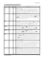
PIN No.
Type
Description
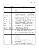
RTS
64
I
Request to send
When the RTS input is forced low, the transmitter starts transmitting the
modem training sequence has been transmitted (signaled by the CTS pin
and CTSB bit becoming active), data present at either the TXDI input pin
in serial mode (PDME bit is reset) or written into the DBFR register in
parallel mode (PDME bit is set) is modulated and transmitted. The RTS
input pin is logically ORed with the RTSB bit in the interface memory.
CTS
78
O
Clear to send
CTS is used to indicate of that the transmission training sequence has
been completed and the modem is ready to transmit any data present at
either the TXID input pin in serial mode (PDME bit is reset) or in DBFR
in parallel mode (PDME bit is set).
RLSD
79
O
Received line signal detector
RLSD becomes active at the end of the reception of the training sequence
indicating the beginning of data reception. If no training is detected but
the received energy level is above the RLSD off-to-on threshold, RLSD
will become active.
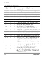
X TALI
68
I
Oscillator In/Out
X TALO 69
O
An
external 24.00014MHz (KS16116) or 38.00053 MHz (KS16117) crystal
and two capacitors are connected to the XTALI and XTALO.
Alternatively, an external crystal oscillator of the appropriate frequency
can be connected to the XTALI input leaving XTALO unconnected.
In order to minimize electromagnetic emissions and ensure proper
oscillator start up and operation, the crystal and the capacitors should be
placed as close as possible to the XTALI and XTALO pins. Further, the
circuit board traces connecting the crystal and capacitors to XTALI and
X TALO should be as short as possible. The use of circuit board bias
should be avoided in the crystal oscillator circuitry and circuit board
traces should be routed using curved turns.
PORI
67
I
Power On reset In
When power is first applied to the modem, PORI is held low for
approximately 350ms. The modem is turn ready for normal operation
15ms after the low to high transition of PORI.
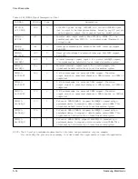
V
D D
22, 72
Power
+5V Digital voltage supply
This pin nust be connected to +5V 5% supply. The +5V Digital power
supply voltage ripple should not exceed 100mV
p-p.
V
cc
46
Power
+5V Analog voltage supply
This pin nust be connected to +5V 5% supply. The +5V Analog power
supply voltage ripple should not exceed 100mV
p-p.
G N D D
6, 7, 16,
G N D
Digital ground
23, 50, 66,
These pins must be connected to digital ground.
77, 80, 81,
89, 92, 97
G N D A
17, 21, G N D
Analog
ground
30, 43, 47
These pins must be connected to analog ground.
Table 2-1 Hardware Interface Signal Descriptions (Cont.)
5-20
Samsung Electronics
Circuit Description
Summary of Contents for MSYS 5150
Page 9: ...2 6 Samsung Electronics Specification Memo ...
Page 16: ...3 26 Samsung Electronics Setup and Installing Memo ...
Page 37: ...4 2 Samsung Electronics Theory of Operation ...
Page 41: ...4 6 Samsung Electronics Memo Theory of Operation ...
Page 116: ...Samsung Electronics 7 9 Maintenance Troubleshooting No Image ...
Page 117: ...Samsung Electronics Maintenance Troubleshooting 7 10 ...
Page 118: ...Samsung Electronics 7 11 Maintenance Troubleshooting All Black ...
Page 119: ...7 12 Samsung Electronics Maintenance Troubleshooting Vertical White Line Band ...
Page 120: ...Samsung Electronics 7 13 Maintenance Troubleshooting Dark Image ...
Page 121: ...7 14 Samsung Electronics Maintenance Troubleshooting Background ...
Page 122: ...Samsung Electronics 7 15 Maintenance Troubleshooting Ghost ...
Page 123: ...7 16 Samsung Electronics Maintenance Troubleshooting Black Dot ...
Page 124: ...Samsung Electronics 7 17 Maintenance Troubleshooting Horizontal Band ...
Page 125: ...7 18 Samsung Electronics Maintenance Troubleshooting Irregular Density ...
Page 126: ...Samsung Electronics 7 19 Maintenance Troubleshooting White Spot ...
Page 127: ...7 20 Samsung Electronics Maintenance Troubleshooting Trembling at the End When OHP Printing ...
Page 128: ...Samsung Electronics 7 21 Maintenance Troubleshooting Poor Fusing Grade ...
Page 132: ...Samsung Electronics 7 25 Maintenance Troubleshooting No Power LCD NO display LED Off ...
Page 133: ...Fuser Error 7 26 Samsung Electronics Maintenance Troubleshooting ...
Page 134: ...Samsung Electronics 7 27 Maintenance Troubleshooting Paper Jam Mis feeding ...
Page 135: ...7 28 Samsung Electronics Maintenance Troubleshooting Paper Jam Jam1 ...
Page 136: ...Samsung Electronics Maintenance Troubleshooting 7 29 Engine Error ...
Page 137: ...7 30 Samsung Electronics Maintenance Troubleshooting Memo ...
Page 187: ...9 28 Samsung Electronics Electrical Parts List ...
Page 189: ...11 Connection Diagram Samsung Electronics 11 1 ...
Page 190: ...12 1 Main Circuit Diagram Samsung Electronics 12 1 12 Schematic Diagrams ...
Page 191: ...Schematic Diagrams 12 2 Samsung Electronics Main Circuit Diagram ...
Page 192: ...Main Circuit Diagram Samsung Electronics 12 3 Schematic Diagrams ...
Page 193: ...Schematic Diagrams 12 4 Samsung Electronics Main Circuit Diagram ...
Page 194: ...Main Circuit Diagram Samsung Electronics 12 5 Schematic Diagrams ...
Page 195: ...Schematic Diagrams 12 6 Samsung Electronics Main Circuit Diagram ...
Page 196: ...Main Circuit Diagram Samsung Electronics 12 7 Schematic Diagrams ...
Page 200: ...12 3 Sensors Circuit Diagram Samsung Electronics 12 11 Schematic Diagrams ...
Page 201: ...Schematic Diagrams 12 12 Samsung Electronics 12 4 Switch Circuit Diagram ...
Page 202: ...Samsung Electronics 12 13 Schematic Diagrams 12 5 Joint Circuit Diagram ...
Page 204: ...Samsung Electronics 12 15 Schematic Diagrams 12 7 PTL Circuit Diagram ...
Page 205: ...Schematic Diagrams 12 16 Samsung Electronics 12 8 SCAN Circuit Diagram ...
Page 206: ...Samsung Electronics 12 17 Schematic Diagrams 12 9 Engin Circuit Diagram ...
Page 207: ...Schematic Diagrams 12 18 Samsung Electronics Engin Circuit Diagram ...
Page 208: ...Samsung Electronics 12 19 Schematic Diagrams 12 10 LIU Circuit Diagram ...
Page 210: ... Samsung Electronics Co Ltd Mar 1999 Printed in Korea P N JC68 00097A Rev 1 00 ELECTRONICS ...


