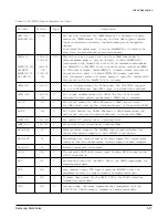
S I G N A L
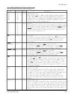
PIN No.
Type
Description
GPIO[11]:
188
O
KS32C6100 power ready. nCPUPWR is a status nCPUPWR signal
n C P U P W R
that is output to the laser printer engine. Actually, any I/O port pin
can be mapped to output this signal without any modifications.
GPIO[10]:
187
O
Parallel data output enable. When PPDOE is PPDOE “1”, the
P P D O E
parallel port data bus, PPD[7:0], is in output mode. Otherwise it is
in input mode.
GPIO[9]:
186 O
Interrupt acknowledge for external ExtiACK1 interrupt request
ExtlACK1
ExitREQ1.
GPIO[8]: 185
O
Interrupt acknowledge for external interrupt ExtiACK0 request
ExtlACK0
ExitREQ0.
GPIO[7]:
182
I
External interrupt request input 1. For a valid ExtiREQ1 request,
ExtlREQ1
this signal must be held active for at least four machine cycles.
GPIO[6]:
181
I
External interrupt request input 0. For a valid request, this
ExtlREQ0
signal must be held active for at least four machine cycles.
GPIO[5]:
180
O
D M A acknowledge for external DMA2 request . The active
ExtDACK2
output signal is generated whenever a DMA transfer on GDMA1 is
completed.
GPIO[4]:
179
O
D M A acknowledge for external DMA1 request . The active
ExtDACK1
output signal is generated whenever a DMA transfer on GDMA0 is
completed.
GPIO[3]:
178
O
D M A acknowledge for external DMA0 request . The active
ExtDACK0
output signal is generated whenever a DMA transfer on GDMA i
s
completed.
GPIO[2]:
177
I
External DMA2(GDMA1) request. ExtDREQ2 is asserted by a
ExtDREQ2
peripheral device to request a data transfer using GDMA1. This
signal must be held active for at least four machine cycles.
GPIO[2]:
176
I
External DMA1(GDMA0) request. ExtDREQ1 is asserted by a
ExtDREQ1
peripheral device to request a data transfer using GDMA0. This
signal must be held active for at least four machine cycles.
GPIO[2]:
175
I
External DMA0(GDMA) request. ExtDREQ0 is asserted by a
ExtDREQ0
peripheral device to request a data transfer using GDMA. This
signal must be held active for at least four machine cycles.
NOTE: The I/O port pin assignments described in this table are presented as only one example.
You can modify the port map as necessary in order to meet the requirements of a specific application.
Table 1-1 KS32C6100 Signal Descriptions (Cont.)
5-14
Samsung Electronics
Circuit Description
Summary of Contents for MSYS 5150
Page 9: ...2 6 Samsung Electronics Specification Memo ...
Page 16: ...3 26 Samsung Electronics Setup and Installing Memo ...
Page 37: ...4 2 Samsung Electronics Theory of Operation ...
Page 41: ...4 6 Samsung Electronics Memo Theory of Operation ...
Page 116: ...Samsung Electronics 7 9 Maintenance Troubleshooting No Image ...
Page 117: ...Samsung Electronics Maintenance Troubleshooting 7 10 ...
Page 118: ...Samsung Electronics 7 11 Maintenance Troubleshooting All Black ...
Page 119: ...7 12 Samsung Electronics Maintenance Troubleshooting Vertical White Line Band ...
Page 120: ...Samsung Electronics 7 13 Maintenance Troubleshooting Dark Image ...
Page 121: ...7 14 Samsung Electronics Maintenance Troubleshooting Background ...
Page 122: ...Samsung Electronics 7 15 Maintenance Troubleshooting Ghost ...
Page 123: ...7 16 Samsung Electronics Maintenance Troubleshooting Black Dot ...
Page 124: ...Samsung Electronics 7 17 Maintenance Troubleshooting Horizontal Band ...
Page 125: ...7 18 Samsung Electronics Maintenance Troubleshooting Irregular Density ...
Page 126: ...Samsung Electronics 7 19 Maintenance Troubleshooting White Spot ...
Page 127: ...7 20 Samsung Electronics Maintenance Troubleshooting Trembling at the End When OHP Printing ...
Page 128: ...Samsung Electronics 7 21 Maintenance Troubleshooting Poor Fusing Grade ...
Page 132: ...Samsung Electronics 7 25 Maintenance Troubleshooting No Power LCD NO display LED Off ...
Page 133: ...Fuser Error 7 26 Samsung Electronics Maintenance Troubleshooting ...
Page 134: ...Samsung Electronics 7 27 Maintenance Troubleshooting Paper Jam Mis feeding ...
Page 135: ...7 28 Samsung Electronics Maintenance Troubleshooting Paper Jam Jam1 ...
Page 136: ...Samsung Electronics Maintenance Troubleshooting 7 29 Engine Error ...
Page 137: ...7 30 Samsung Electronics Maintenance Troubleshooting Memo ...
Page 187: ...9 28 Samsung Electronics Electrical Parts List ...
Page 189: ...11 Connection Diagram Samsung Electronics 11 1 ...
Page 190: ...12 1 Main Circuit Diagram Samsung Electronics 12 1 12 Schematic Diagrams ...
Page 191: ...Schematic Diagrams 12 2 Samsung Electronics Main Circuit Diagram ...
Page 192: ...Main Circuit Diagram Samsung Electronics 12 3 Schematic Diagrams ...
Page 193: ...Schematic Diagrams 12 4 Samsung Electronics Main Circuit Diagram ...
Page 194: ...Main Circuit Diagram Samsung Electronics 12 5 Schematic Diagrams ...
Page 195: ...Schematic Diagrams 12 6 Samsung Electronics Main Circuit Diagram ...
Page 196: ...Main Circuit Diagram Samsung Electronics 12 7 Schematic Diagrams ...
Page 200: ...12 3 Sensors Circuit Diagram Samsung Electronics 12 11 Schematic Diagrams ...
Page 201: ...Schematic Diagrams 12 12 Samsung Electronics 12 4 Switch Circuit Diagram ...
Page 202: ...Samsung Electronics 12 13 Schematic Diagrams 12 5 Joint Circuit Diagram ...
Page 204: ...Samsung Electronics 12 15 Schematic Diagrams 12 7 PTL Circuit Diagram ...
Page 205: ...Schematic Diagrams 12 16 Samsung Electronics 12 8 SCAN Circuit Diagram ...
Page 206: ...Samsung Electronics 12 17 Schematic Diagrams 12 9 Engin Circuit Diagram ...
Page 207: ...Schematic Diagrams 12 18 Samsung Electronics Engin Circuit Diagram ...
Page 208: ...Samsung Electronics 12 19 Schematic Diagrams 12 10 LIU Circuit Diagram ...
Page 210: ... Samsung Electronics Co Ltd Mar 1999 Printed in Korea P N JC68 00097A Rev 1 00 ELECTRONICS ...

