5-26
Samsung Electronics
Circuit Description
5-3 OPE PBA
5-3-1 SUMMARY
OPE Board is separated functionally from the main
board and operated by the micom(Z8601) in the
board. OPE and the main use UART (universal
asynchronous receiver/transmitter) channel to
exchange information. OPE reset can be controlled by
the main. OPE micom controls key-scanning and LCD
and LED display, detects documents and
senses SCAN position. If there occurs an event in OPE
(such as key touch and sensor level change), it sends
specific codes to the main to respond to the situation
and the main analyzes these codes and operates the
system. For example, if the main is to display
messages in OPE, the main transmits data through
U A RT line to OPE according to the
designated format and OPE displays this on LCD,
LED. OPE’s sensing is also transmitted to the main
through UART line and then the main drives
necessary operation.
5-3-2
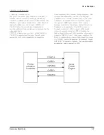
OPE PBA consists of U1 (MICOM, Z8601), LCD, key
matrix, LED indicators, SCAN position sensor and the
document detect sensor. Refer to OPE Schematic
Diagram and Wiring Diagram sections of this manual.
• Signals
from the key matrix are delivered to U1X/Y
input pin group (P1-x).
• U1 pin 4 (TX D ATA) is the UART code sent to
MAIN PBA.
• Display from the controller is received at U1 pin 5
(RX DATA).
• LCD drive signals are sent from U1 P2-x pin group,
P3-4~P3-6 pins.
• Machine status LED drive signals are sent from U1
P0-x pin group.
• Document detect sensor output is received at U1
pin 33 (P3-3).
• Scan position sensor output is received at U1 pin 43
(P3-1).
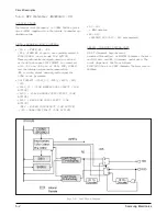
OPE BLOCK DIAGRAM
Summary of Contents for MSYS 5150
Page 9: ...2 6 Samsung Electronics Specification Memo ...
Page 16: ...3 26 Samsung Electronics Setup and Installing Memo ...
Page 37: ...4 2 Samsung Electronics Theory of Operation ...
Page 41: ...4 6 Samsung Electronics Memo Theory of Operation ...
Page 116: ...Samsung Electronics 7 9 Maintenance Troubleshooting No Image ...
Page 117: ...Samsung Electronics Maintenance Troubleshooting 7 10 ...
Page 118: ...Samsung Electronics 7 11 Maintenance Troubleshooting All Black ...
Page 119: ...7 12 Samsung Electronics Maintenance Troubleshooting Vertical White Line Band ...
Page 120: ...Samsung Electronics 7 13 Maintenance Troubleshooting Dark Image ...
Page 121: ...7 14 Samsung Electronics Maintenance Troubleshooting Background ...
Page 122: ...Samsung Electronics 7 15 Maintenance Troubleshooting Ghost ...
Page 123: ...7 16 Samsung Electronics Maintenance Troubleshooting Black Dot ...
Page 124: ...Samsung Electronics 7 17 Maintenance Troubleshooting Horizontal Band ...
Page 125: ...7 18 Samsung Electronics Maintenance Troubleshooting Irregular Density ...
Page 126: ...Samsung Electronics 7 19 Maintenance Troubleshooting White Spot ...
Page 127: ...7 20 Samsung Electronics Maintenance Troubleshooting Trembling at the End When OHP Printing ...
Page 128: ...Samsung Electronics 7 21 Maintenance Troubleshooting Poor Fusing Grade ...
Page 132: ...Samsung Electronics 7 25 Maintenance Troubleshooting No Power LCD NO display LED Off ...
Page 133: ...Fuser Error 7 26 Samsung Electronics Maintenance Troubleshooting ...
Page 134: ...Samsung Electronics 7 27 Maintenance Troubleshooting Paper Jam Mis feeding ...
Page 135: ...7 28 Samsung Electronics Maintenance Troubleshooting Paper Jam Jam1 ...
Page 136: ...Samsung Electronics Maintenance Troubleshooting 7 29 Engine Error ...
Page 137: ...7 30 Samsung Electronics Maintenance Troubleshooting Memo ...
Page 187: ...9 28 Samsung Electronics Electrical Parts List ...
Page 189: ...11 Connection Diagram Samsung Electronics 11 1 ...
Page 190: ...12 1 Main Circuit Diagram Samsung Electronics 12 1 12 Schematic Diagrams ...
Page 191: ...Schematic Diagrams 12 2 Samsung Electronics Main Circuit Diagram ...
Page 192: ...Main Circuit Diagram Samsung Electronics 12 3 Schematic Diagrams ...
Page 193: ...Schematic Diagrams 12 4 Samsung Electronics Main Circuit Diagram ...
Page 194: ...Main Circuit Diagram Samsung Electronics 12 5 Schematic Diagrams ...
Page 195: ...Schematic Diagrams 12 6 Samsung Electronics Main Circuit Diagram ...
Page 196: ...Main Circuit Diagram Samsung Electronics 12 7 Schematic Diagrams ...
Page 200: ...12 3 Sensors Circuit Diagram Samsung Electronics 12 11 Schematic Diagrams ...
Page 201: ...Schematic Diagrams 12 12 Samsung Electronics 12 4 Switch Circuit Diagram ...
Page 202: ...Samsung Electronics 12 13 Schematic Diagrams 12 5 Joint Circuit Diagram ...
Page 204: ...Samsung Electronics 12 15 Schematic Diagrams 12 7 PTL Circuit Diagram ...
Page 205: ...Schematic Diagrams 12 16 Samsung Electronics 12 8 SCAN Circuit Diagram ...
Page 206: ...Samsung Electronics 12 17 Schematic Diagrams 12 9 Engin Circuit Diagram ...
Page 207: ...Schematic Diagrams 12 18 Samsung Electronics Engin Circuit Diagram ...
Page 208: ...Samsung Electronics 12 19 Schematic Diagrams 12 10 LIU Circuit Diagram ...
Page 210: ... Samsung Electronics Co Ltd Mar 1999 Printed in Korea P N JC68 00097A Rev 1 00 ELECTRONICS ...


