


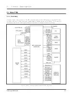


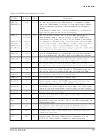


Circuit Description
Samsung Electronics
5-3
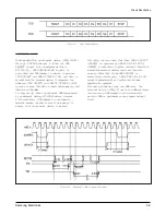
Fig.5-3. Uart Data Format
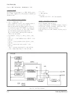
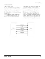
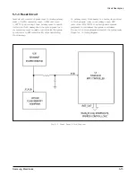
Fig.5-4. External DMA Timing Diagram
EXTERNAL D M A
It brings data from an external device (SCAN_IP:U31)
through EXTDMA channel 1. When the DMA
REQUEST is sent from an external device to
KS32C6100, DMA ACKNOWLEDGE signal is
activated and DMA channel 1 is driven to produce
CHIP SELECT and READ STROBE (/RD) and data is
brought from the external device. It generates the
address, CHIP SELECT and WRITE STROBE (/WR)
in order to move this data to destination memory, and
then stores the data.
In other words, when the external DMA is requested
by an external device, KS32C6100 drives internal
D M A controller, DMA channel 1 is assigned to
external channel, the data is sent from memory to
memory or from external device to memory.
Following timing shows that when DMA REQUEST
(/XDREQ) is generated, DMA A C K N O W L E D G E
(/XDACK) is sent after 2 cycles and the 2 Word Data
is read from external device, and is written into
memory.
After that if the DMA REQUEST is
maintained continuously, DMA A C K N O W L E D G E
signal is generated after 4 cycles and the same
operation is repeated.
Following diagram shows one DMA cycle. The
external device (SCAN_IP) using the DMA maintains
continuously DMA request to be activated until
second DMA is performed, so one request brings 2
W ord.
Summary of Contents for MSYS 5150
Page 9: ...2 6 Samsung Electronics Specification Memo ...
Page 16: ...3 26 Samsung Electronics Setup and Installing Memo ...
Page 37: ...4 2 Samsung Electronics Theory of Operation ...
Page 41: ...4 6 Samsung Electronics Memo Theory of Operation ...
Page 116: ...Samsung Electronics 7 9 Maintenance Troubleshooting No Image ...
Page 117: ...Samsung Electronics Maintenance Troubleshooting 7 10 ...
Page 118: ...Samsung Electronics 7 11 Maintenance Troubleshooting All Black ...
Page 119: ...7 12 Samsung Electronics Maintenance Troubleshooting Vertical White Line Band ...
Page 120: ...Samsung Electronics 7 13 Maintenance Troubleshooting Dark Image ...
Page 121: ...7 14 Samsung Electronics Maintenance Troubleshooting Background ...
Page 122: ...Samsung Electronics 7 15 Maintenance Troubleshooting Ghost ...
Page 123: ...7 16 Samsung Electronics Maintenance Troubleshooting Black Dot ...
Page 124: ...Samsung Electronics 7 17 Maintenance Troubleshooting Horizontal Band ...
Page 125: ...7 18 Samsung Electronics Maintenance Troubleshooting Irregular Density ...
Page 126: ...Samsung Electronics 7 19 Maintenance Troubleshooting White Spot ...
Page 127: ...7 20 Samsung Electronics Maintenance Troubleshooting Trembling at the End When OHP Printing ...
Page 128: ...Samsung Electronics 7 21 Maintenance Troubleshooting Poor Fusing Grade ...
Page 132: ...Samsung Electronics 7 25 Maintenance Troubleshooting No Power LCD NO display LED Off ...
Page 133: ...Fuser Error 7 26 Samsung Electronics Maintenance Troubleshooting ...
Page 134: ...Samsung Electronics 7 27 Maintenance Troubleshooting Paper Jam Mis feeding ...
Page 135: ...7 28 Samsung Electronics Maintenance Troubleshooting Paper Jam Jam1 ...
Page 136: ...Samsung Electronics Maintenance Troubleshooting 7 29 Engine Error ...
Page 137: ...7 30 Samsung Electronics Maintenance Troubleshooting Memo ...
Page 187: ...9 28 Samsung Electronics Electrical Parts List ...
Page 189: ...11 Connection Diagram Samsung Electronics 11 1 ...
Page 190: ...12 1 Main Circuit Diagram Samsung Electronics 12 1 12 Schematic Diagrams ...
Page 191: ...Schematic Diagrams 12 2 Samsung Electronics Main Circuit Diagram ...
Page 192: ...Main Circuit Diagram Samsung Electronics 12 3 Schematic Diagrams ...
Page 193: ...Schematic Diagrams 12 4 Samsung Electronics Main Circuit Diagram ...
Page 194: ...Main Circuit Diagram Samsung Electronics 12 5 Schematic Diagrams ...
Page 195: ...Schematic Diagrams 12 6 Samsung Electronics Main Circuit Diagram ...
Page 196: ...Main Circuit Diagram Samsung Electronics 12 7 Schematic Diagrams ...
Page 200: ...12 3 Sensors Circuit Diagram Samsung Electronics 12 11 Schematic Diagrams ...
Page 201: ...Schematic Diagrams 12 12 Samsung Electronics 12 4 Switch Circuit Diagram ...
Page 202: ...Samsung Electronics 12 13 Schematic Diagrams 12 5 Joint Circuit Diagram ...
Page 204: ...Samsung Electronics 12 15 Schematic Diagrams 12 7 PTL Circuit Diagram ...
Page 205: ...Schematic Diagrams 12 16 Samsung Electronics 12 8 SCAN Circuit Diagram ...
Page 206: ...Samsung Electronics 12 17 Schematic Diagrams 12 9 Engin Circuit Diagram ...
Page 207: ...Schematic Diagrams 12 18 Samsung Electronics Engin Circuit Diagram ...
Page 208: ...Samsung Electronics 12 19 Schematic Diagrams 12 10 LIU Circuit Diagram ...
Page 210: ... Samsung Electronics Co Ltd Mar 1999 Printed in Korea P N JC68 00097A Rev 1 00 ELECTRONICS ...