LCC/LGA Module Series
Module Secondary SMT User Guide
Module_Secondary_SMT_User_Guide 18 / 25
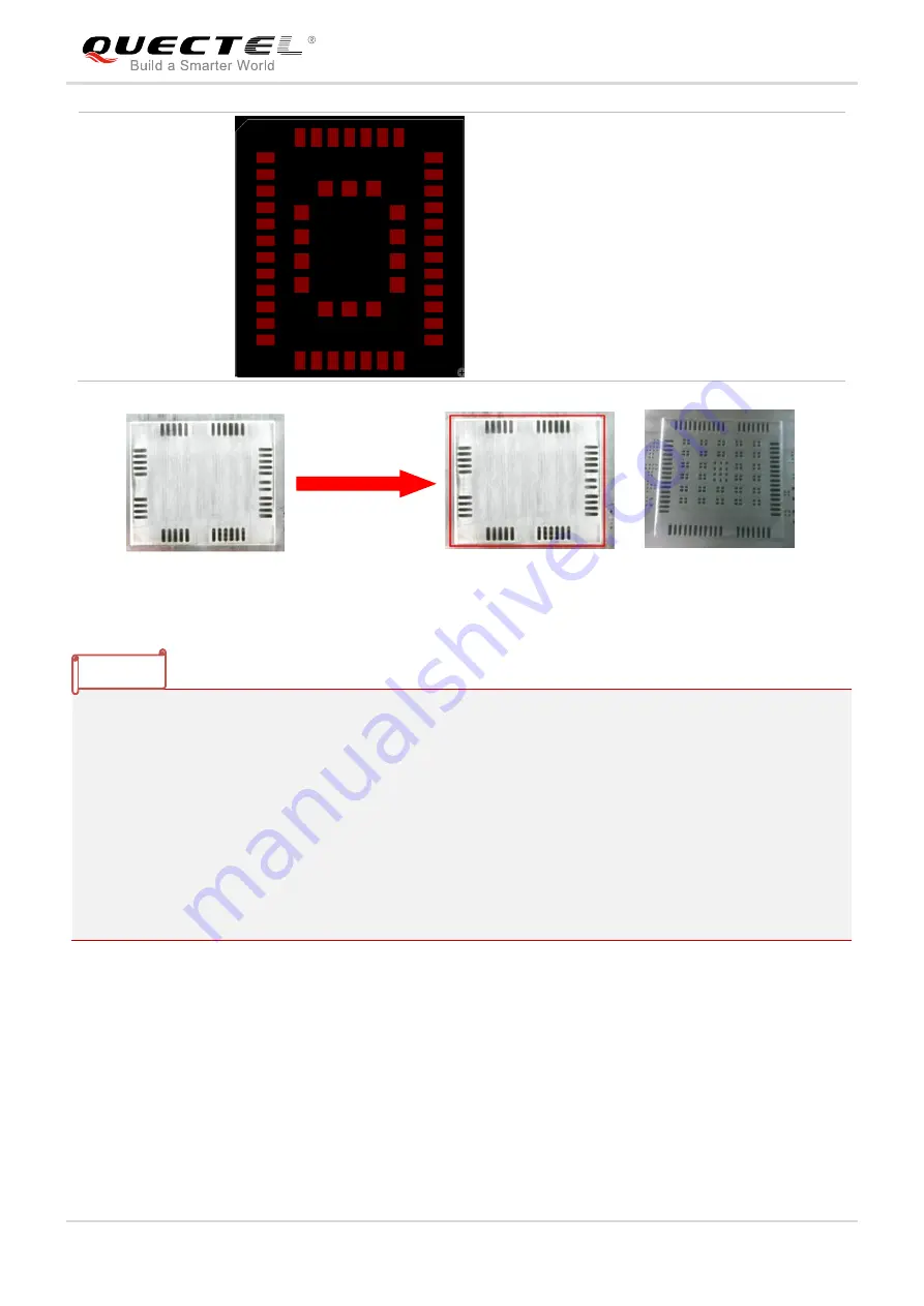
AF20
1. The stencil thickness of the area for the
module should be partly stepped-up to
0.13-0.15mm.
2. For pads on four sides:
The stencil aperture for each pad should
be centered with area reduced to
75%-85% and the shape should be
rectangle with round chamfers.
3. For square pads in the center:
The stencil aperture should be designed
into round with area reduced to 70%.
Figure 3: Step-up Stencil Area
1.
“*” means under development.
2. Area of the stencil apertures for components within 1mm from the thickened stencil part should be
reduced by 10%-30% compared with regular apertures, since the thickening will increase the volume
of solder paste. For components with 0.5mm pitch (or smaller) or 0201 components, please keep at
least 3mm space in between, otherwise there may be a risk of solder bridging that will cause short
circuit of the component.
3. You can optimize the stencil design depending on the actual situation.
4. Inward shrinking and outward extending are relative to the host PCB footprint of the module. For
details of the recommended footprint, please refer to the hardware designs of corresponding
modules.
4.3. Mounting Process
4.3.1. Load Materials
In order to ensure mounting accuracy, for single modules that have been unpacked for baking, it is
recommended for the customers to use a dedicated tray/fixture for module loading.
NOTES


