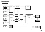
No signal
With signal
Signal direction
Main power ON
(POWER button ON)
★
Pin No.
Pin name
Function
Standby
★★★
Power
management
★★
Main power
OFF
★★
AC power OFF
(Power cord
pulled out of
the wall outlet)
★★
AC power ON
(Power cord
connected to
the wall outlet)
★★
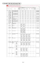
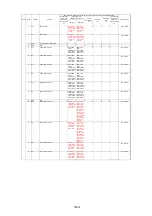
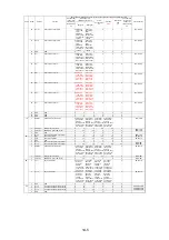
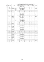
Basic operation (Numerical unit: Vdc; except for the case when units are individually indicated)
Name
42VR5
42XR3
50XR4
61XR3
0
0
0
0
0
0
-
11
232C_SHUT ON/OFF control for TXD0 driver
0
3.3
3.3
3.3
3.3
0
-
MAIN
→
RS232C
12
REM
Insertion
detection for
wired remote
control input
42VM5
42VP5
42XM3
50XM4
61XM3
0 3.3V when a
wired remote
control is
connected/
When not
connected.
3.3V when a
wired remote
control is
connected/
When not
connected.
3.3V when a
wired remote
control is
connected/
When not
connected.
3.3V when a
wired remote
control is
connected/
When not
connected.
0
-
RS232C
→
MAIN
42VR5
42XR3
50XR4
61XR3
-
-
-
-
-
-
- (NC for Model R)
TM
1
SCL5
Clock line of the I2C bus
0 Clock signal
used during
data
transmission
(3.3Vac)
3.3Vdc when
no data are
transmitted.
Clock signal
used during
data
transmission
(3.3Vac)
3.3Vdc when
no data are
transmitted.
0
0
0
-
MAIN
→
SENB
2
GND
GND
0
0
0
0
0
0
-
-
3
VDD+3.3V
3.3V power supply for analog signals
0
3.3
3.3
0
0
0
-
MAIN
→
SENB
4
SDA5
Data line of the I2C bus
0 During data
exchange:
Clock signal
(3.3Vac), Data
not
exchanged:
3.3Vdc
During data
exchange:
Clock signal
(3.3Vac), Data
not
exchanged:
3.3Vdc
0
0
0
-
MAIN
←→
SENB
TR
1
SCL5
Clock line of the I2C bus
0 Clock signal
used during
data
transmission
(3.3Vac)
3.3Vdc when
no data are
transmitted.
Clock signal
used during
data
transmission
(3.3Vac)
3.3Vdc when
no data are
transmitted.
0
0
0
-
SENB
→
SEN
D
2
GND
GND
0
0
0
0
0
0
-
-
3
VDD+3.3V
3.3V power supply for analog signals
0
3.3
3.3
0
0
0
-
SENB
→
SEN
D
4
SDA5
Data line of the I2C bus
0 During data
exchange:
Clock signal
(3.3Vac), Data
not
exchanged:
3.3Vdc
During data
exchange:
Clock signal
(3.3Vac), Data
not
exchanged:
3.3Vdc
0
0
0
-
SENB
←→
SEND
TS
1
SCL5
Clock line of the I2C bus
0 Clock signal
used during
data
transmission
(3.3Vac)
3.3Vdc when
no data are
transmitted.
Clock signal
used during
data
transmission
(3.3Vac)
3.3Vdc when
no data are
transmitted.
0
0
0
-
SEND
→
SENC
2
GND
GND
0
0
0
0
0
0
-
-
3
VDD+3.3V
3.3V power supply for analog signals
0
3.3
3.3
0
0
0
-
SEND
→
SENC
4
SDA5
Data line of the I2C bus
0 During data
exchange:
Clock signal
(3.3Vac), Data
not
exchanged:
3.3Vdc
During data
exchange:
Clock signal
(3.3Vac), Data
not
exchanged:
3.3Vdc
0
0
0
-
SEND
←→
SENC
FA
1
FAN-CTL
Voltage-
controllable
power supply
42VM5
42VP5
42VR5
-
-
-
-
-
-
-
-
42XM3
42XR3
0 11.5Vdc
during high-
speed
revolution
(Fan mode H);
8.5Vdc during
medium speed
revolution
(Fan mode M);
6.5Vdc during
low-speed
revolution
(Fan mode L)
11.5Vdc
during high-
speed
revolution
(Fan mode H);
8.5Vdc during
medium speed
revolution
(Fan mode M);
6.5Vdc during
low-speed
revolution
(Fan mode L)
0
0
0
-
MAIN
→
FAN
50XM4
50XR4
0 11.6Vdc
during high-
speed
revolution
(Fan mode H);
7.8Vdc during
medium speed
revolution
(Fan mode M);
5.3Vdc during
low-speed
revolution
(Fan mode L)
11.6Vdc
during high-
speed
revolution
(Fan mode H);
7.8Vdc during
medium speed
revolution
(Fan mode M);
5.3Vdc during
low-speed
revolution
(Fan mode L)
0
0
0
-
61XM3
61XR3
0 9.3Vdc during
high-speed
revolution
(Fan mode H);
7.6Vdc during
medium speed
revolution
(Fan mode M);
5.3Vdc during
low-speed
revolution
(Fan mode L)
9.3Vdc during
high-speed
revolution
(Fan mode H);
7.6Vdc during
medium speed
revolution
(Fan mode M);
5.3Vdc during
low-speed
revolution
(Fan mode L)
0
0
0
-
2
GND
GND
0
0
0
0
0
0
-
-
3
ALARM
42VM5
42VP5
42VR5
-
-
-
-
-
-
-
-
FAN lock detect
signal output
14-2
Summary of Contents for Elite PureVision PRO 1410HD
Page 5: ...2 3 ...
Page 6: ...2 4 ...
Page 8: ...SPECIFICATIONS PDP 614MX 3 1 ...
Page 9: ... PRO 1410HD 3 2 ...
Page 10: ...TABLE OF SIGNAL SUPPORTED PDP 614MX 4 1 ...
Page 11: ...4 2 ...
Page 12: ...4 3 PRO 1410HD ...
Page 13: ...4 4 ...
Page 14: ...PANEL FACILITIES 5 1 PDP 614MX ...
Page 15: ...5 2 ...
Page 16: ...5 3 PRO 1410HD ...
Page 17: ...5 4 ...
Page 32: ...7 11 ...
Page 44: ...All white signal All white signal 8 12 ...
Page 50: ... Fig 1 CCD PWB Pattern Diagram A B D E 3 3V 6V C 8 18 ...
Page 51: ...8 19 Check point MAIN PWB ...
Page 52: ...8 20 232C PWB ...
Page 53: ...8 21 CLT PWB ...
Page 54: ...8 22 PWR PWB ...
Page 55: ...8 23 LED PWB ...
Page 56: ...8 24 SENB PWB ...
Page 57: ...8 25 SENC PWB ...
Page 58: ...8 26 SEND PWB ...
Page 59: ...AUDIO PWB 8 27 ...
Page 60: ...8 28 CCD PWB PX A only ...

