background image

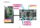
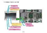
(1)SRW16 SCREW(UNC4-40/4-40)

32990229  *4p

(1)SRW16 SCREW(UNC4-40/4-40)

32990229  *4p

(6)A01 MAIN 1  PWB ASSY

(6)A01 MAIN 1  PWB ASSY

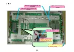
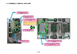
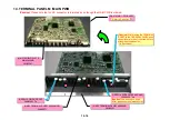
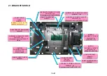
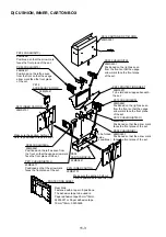
14. TERMINAL PANEL M /MAIN PWB

(Caution) 

Use a hexagon head 

driver (opposite side distance 5mm).

(Caution) 

Use a hexagon head 

driver (opposite side distance 5mm).

(Caution) 

Please note that no DS connector is furnished even though the MAIN PWB is ordered.

Refer to Parts List

Refer to Parts List

(5)M27 SHIELD PLATE 

MAIN(42XM3)

29H03541

(5)M27 SHIELD PLATE 

MAIN(42XM3)

29H03541

(3)M52 TERMINAL SHEET M(50XM3)W

29K00571

(3)M52 TERMINAL SHEET M(50XM3)W

29K00571

(2)SRW15 CBIPS*3*8*3KF

24N03691 *7p

(2)SRW15 CBIPS*3*8*3KF

24N03691 *7p

(4)M28 TERMINAL PANEL M(50XM3)

29H02551

(4)M28 TERMINAL PANEL M(50XM3)

29H02551

(Caution) 

After sticking the TERMINAL 

SHEET to the TERMINAL PANEL, push 

the peripheral area of the screw hole to 

strengthen the adhesion.

(In 3 positions)

(Caution) 

After sticking the TERMINAL 

SHEET to the TERMINAL PANEL, push 

the peripheral area of the screw hole to 

strengthen the adhesion.

(In 3 positions)

10-14

Summary of Contents for Elite PureVision PRO 1410HD

Page 1: ... Keetberglaan 1 9120 Melsele Belgium PIONEER ELECTRONICS ASIACENTRE PTE LTD 253 Alexandra Road 04 01 Singapore 159936 PIONEER CORPORATION 2004 ARP3232 PLASMA DISPLAY PDP 614MXLUC T ZZE NOV 2004 Printed in Japan PRO 1410HDLUC PDP 614MX THIS MANUAL IS APPLICABLE TO THE FOLLOWING MODEL S AND TYPE S Model Type Power Requirement Remarks PDP 614MX LUC AC100 120V PRO 1410HD LUC AC120V ...

Page 2: ... 1 PANEL FACILITIES 5 1 CONTRAST OF MISCELLANEOUS PARTS 6 1 HOW TO DIAGNOSE THE PDP MODULE 7 1 TROUBLESHOOTING 8 1 METHOD OF ADJUSTMENTS 9 1 METHOD OF DISASSEMBLY 10 1 METHOD OF PACKAGING 11 1 PARTS LIST 12 1 CONNECTION DIAGRAMS 13 1 CONNECTOR PIN EXPLANATION 14 1 BLOCK DIAGRAM 15 1 ...

Page 3: ...mpartment covershields isolation resistor capacitor etc 3 When service is required observe the original lead dress Extra precaution should be taken to assure correct lead dress in the high voltage circuitry area 4 Always use the manufacture s replacement components Especially critical components as indicated on the circuit diagram should not be replaced by other manufacture s Furthermore where a s...

Page 4: ...must not exceed 0 5mA ANY MEASUREMENTS NOT WITHIN THE LIMITS OUTLINED ABOVE ARE INDICATIVE OF A POTENTIAL SHOCK HAZARD AND MUST BE CORRECTED BEFORE RETURNING THE SET TO THE CUSTOMER PRODUCT SAFETY NOTICE Many electrical and mechanical parts in PIONEER set have special safety related characteristics These are often not evident from visual inspection nor the protection afforded by them necessarily c...

Page 5: ...2 3 ...

Page 6: ...2 4 ...

Page 7: ...eck that neither solder debris nor screws remain inside the product 8 There should be no semi broken wires scratches melting etc on the coating of the power cord Damaged power cords may lead to fire accidents so please be sure that there are no damages If you find a damaged power cord please exchange it with a suitable one 9 There should be no spark traces or similar marks on the power plug When s...

Page 8: ...SPECIFICATIONS PDP 614MX 3 1 ...

Page 9: ... PRO 1410HD 3 2 ...

Page 10: ...TABLE OF SIGNAL SUPPORTED PDP 614MX 4 1 ...

Page 11: ...4 2 ...

Page 12: ...4 3 PRO 1410HD ...

Page 13: ...4 4 ...

Page 14: ...PANEL FACILITIES 5 1 PDP 614MX ...

Page 15: ...5 2 ...

Page 16: ...5 3 PRO 1410HD ...

Page 17: ...5 4 ...

Page 18: ...ONTROL BUTTON G Not used 29G00401 M50 INDICATOR 50XM3 29K00421 Not used M52 TERMINAL SHEET M 50XM3 W 29K00571 Not used M52 TERMINAL SHEET M 614MX Not used 29K00711 M53 TERMINAL SHEET S 50XM3 W 29K00581 Not used M53 TERMINAL SHEET S 614MX Not used 29K00721 M54 FILTER 61A 29KS0211 Not used M54 FILTER 61B Not used 29KS0171 M57 NSP NAME PLATE 61XM3A 29L05811 Not used M57 NSP NAME PLATE PDP 614MX Not u...

Page 19: ...OTICE SHEET US PDP 78038622 Not used PK14 CARTON BOX 61XM3 29MS3091 Not used PK14 CARTON BOX T PDP 614MX Not used 29M01051 PK16 REM T HAND UNIT RP 114 3S120221 Not used PK16 REM T HAND UNIT AXD1498 Not used 3S120241 PK31 NSP MODEL NAME LABEL 29L05951 Not used PK33 POWER CORD CASE Not used 29MS3241 Symbol Mark Symbol and Description Remarks PX 61XM3A PDP 614MX LUC Part No 6 2 ...

Page 20: ...01 M16 FRONT PANEL 61XM2 29D00612 Not used M28 TERMINAL PANEL M 50XM3 29H02551 Not used M28 TERMINAL PANEL M 50XR4 Not used 29H03491 M50 INDICATOR 50XM3 29K00421 Not used M52 TERMINAL SHEET M 50XM3 W 29K00571 Not used M52 TERMINAL SHEET M ELITE Not used 29K00731 M53 TERMINAL SHEET S 50XM3 W 29K00581 Not used M53 TERMINAL SHEET S ELITE Not used 29K00741 M54 FILTER 61A 29KS0211 Not used M54 FILTER 6...

Page 21: ...C 29MS2651 Not used PK09 CUSHION BC E Not used 29MS3201 PK10 CUSHION BR 29MS2661 Not used PK10 CUSHION BR E Not used 29MS3211 PK11 CUSHION BTM L 29MS2671 Not used PK11 CUSHION BTM L E Not used 29MS3221 PK12 CUSHION BTM R 29MS2681 Not used PK12 CUSHION BTM R E Not used 29MS3231 PK14 CARTON BOX 61XM3 29MS3091 Not used PK14 CARTON BOX T PRO 1410HD Not used 29M01071 PK16 REM T HAND UNIT RP 114 3S12022...

Page 22: ...lips screwdriver For detaching reattaching PKGs b Antistatic wrist strap To be used when electronic components such as PKGs are to be handled c Signal generator PC etc For voltage adjustment and display check d Powe For voltage adjustment and display check f Tester For cable check voltage adjustment etc g Cushion To be used when the PKGs are to be replaced Note Be sure to wear a wrist strap when y...

Page 23: ...ter of the Scanning PKG Approx 10 Ω 1 W Fusible resistor R29 located at the upper left corner of the Scanning PKG Approx 4 7 Ω 1 4 W Fusible resistor R108A located at the lower right corner of the Scanning PKG Approx 2 2 Ω 1 W Fusible resistor R113 located at the lower right corner of the Scanning PKG Aapprox 4 7 Ω 2 W PH2311 rear view PH2312 rear view 1 A 14 15 D 58 62 A 59 62 B 54 57 C 46 E 42 G...

Page 24: ...n the Scanning Relay PKG is in failure Failure diagnosis of the Common PKG Glass fuses F1 and F2 at the upper right corner of the Common PKG Fusible resistor R101 at the lower right corner of the Common PKG Approx 2 2 Ω 1 W A 13 16 B 23 26 C 28 31 D 58 62 E 53 56 F 47 51 G 42 45 H 37 40 I 32 35 Check points Check points Between A and B Between B and H Between C and I Between D and E Between F and ...

Page 25: ...e symptom The image in any block of the screen is not displayed Chip fuse FU701 at the upper right corner of the digital PKG CN2 CN3 CN8 CN8 CN8 CN8 CN8 CN2 CN3 Check with a tester between Pin 5 or 6 Vd line of Data IC and ground of each Signal Relay PKG Failure diagnosis of the Digital PKG 7 4 ...

Page 26: ...ectors Scanning PKG 8 connectors Common Branch PKG lower One connector Signal Relay PKG upper left 7 connectors Signal Relay PKG upper center 10 connectors Signal Relay PKG upper right 8 connectors Signal Relay PKG lower right 8 connectors Signal Relay PKG lower center 10 connectors Signal Relay PKG lower left 8 connectors Scanning Relay PKG upper 5 connectors Scanning Relay PKG lower 5 connectors...

Page 27: ...KG lower One screw Signal Relay PKG upper left 4 screws Signal Relay PKG upper center 5 screws Signal Relay PKG upper right 5 screws Signal Relay PKG lower right 5 screws Signal Relay PKG lower center 5 screws Signal Relay PKG lower left 4 screws Signal Relay PKG upper left 7 connectors Common board 10 connectors Scanning PKG 8 connectors Signal Relay PKG upper center 10 connectors Signal Relay PK...

Page 28: ...lay PKG photo and Digital PKG Between the Signal Relay PKG and Digital PKG photo Between the panel and Common PKG photo Between the Scanning PKG photo and Recovery Relay PKG Between the Signal Relay PKG and Scanning PKG photo Between the Scanning Relay PKG photo and panel Between the Scanning PKG photo and Signal Relay PKG photo 7 7 ...

Page 29: ...inside the Common PKG Points to measure Voltage between TP10 and GND chassis GND on the Common PKG Adjustment method Adjust VR101 so that the Vsw value of TP10 becomes in the range of 0 5 V of the Vsw value indicated on the drive voltage label Vbw Vsw Vp s185 0 d65 0 115 2 209 9 199 8 311200062 Vbw Vsw Vp s185 0 d65 0 115 2 209 9 199 8 311200062 V Example bw 115 2V Vsw 209 9V Vp 199 8V Common PKG ...

Page 30: ...ue of TP32 becomes in the range of 1 5 V of the Vp value indicated on the drive voltage label Vbw adjustment inside the Scanning PKG Points to measure Voltage between TP34 and GND chassis GND on the Scanning PKG Adjustment method Adjust VR2 so that the Vbw value of TP34 becomes in the range of 0 5 V of the Vbw value indicated on the drive voltage label Scanning PKG Scanning PKG 7 9 ...

Page 31: ...lly white screen After that check the screen by displaying a fully red fully green and fully blue screen color bars and gray scale Note If any flashing or luminescent spots are recognized during display check after a long period of storage of the module perform aging with a fully white screen displayed for another hour or so 7 10 ...

Page 32: ...7 11 ...

Page 33: ...tures available 2 Go to Image errors P8 8 No video loop out signal is generated The MAIN PWB is faulty Remote control not effective 3 Go to Audio errors P8 14 Remote control not effective 4 Go to Remote control not effective P8 15 The closed caption is displayed incorrectly PX A only 5 Go to The closed caption CC is displayed incorrectly P8 17 8 1 TROUBLESHOOTING ...

Page 34: ... in green and then in red Alarm of power line error Go to P8 7 Is a 5Vdc output available in the state that the LD connector is disconnected and the main power is turned ON The LD connector or the LED PWB is fault YES NO Is a 5Vdc output available in the state that the RS connector is disconnected and the main power is turned ON The RS connector or the 232C PWB is fault YES NO The PW connector PWR...

Page 35: ...he SENB PWB is fault NO The MAIN PWB is fault Is there a display of for all the numerals at the right side of T1 T2 T3 NO YES Press the remove control keys in the sequential order of POWER ON POWER ON EXIT DISPLAY and enter the factory adjustment menu Press the MENU ENTER key to display the FAN SET menu P2 11 Blinking in green intervals of 2 seconds FAN SET Turn off the main power supply Pressing ...

Page 36: ... for the 61XM3 Series The MAIN PWB is fault Is the fan running Caution When alarming is canceled FAN MODE of FAN SET P2 11 in the factory adjustment menu automatically moves from ENA to H thus causing the fan to run Is there a 3 3Vdc output at Pin of the FA and FB FC connectors Is there a voltage output of 11 3Vdc for PX 42XM3 XR3 11 2Vdc for PX 50XM4 XR4 and 9 3Vdc for PX 61XM3 XR3 respectively w...

Page 37: ...y 1 Turn off the main power supply and pull out the power cord from the wall outlet 2 Wait for about 60 minutes until the temperature in the main unit lowers 3 Check whether the heat discharge port is covered with dust or the like If yes remove the clogging substance 4 If the unit is used where the ambient temperature is high it should be moved to an adequate place air temperature ranging from 5 C...

Page 38: ...ied below Caution When the main power supply is turned on with the Menu key of the product kept pressed it takes 30 seconds more to assume the state of blinking in red and green In this time period the following voltage checks should be carried out If the state of blinking in red and green is assumed during this checking take actions of Alarm Canceling and Voltage Check Mode Setup again YES The PD...

Page 39: ... the AUDIO PWB is fault The Power unit or the PN connector is fault Caution The voltage values of Vd and Vs can differ according to the PDP The method of checking these voltage values is obtainable from 2 Adjustment of the power unit in the method of adjustment YES The MAIN PWB is fault Make an OFF ON setting twice for the main power supply in order to reset the alarming condition Is the LED lit i...

Page 40: ...ioration in brightness 2 Failure in writing All whitesignal No signal This is not a fault Failure in writing Deterioration in brightness This is not a fault A Dot errors change with no continuity The PDP is fault All whitesignal All whitesignal Refer to P7 1 HOW TO DIAGNOSE THE PDP MODULE Residual images are seen without signal entry 8 8 ...

Page 41: ...ghting The PDP is fault The images are dark even with an all white input The PDP is fault Line defect The PDP is fault All black signal All black signal Dot errors change with no continuity All white signal Refer to P7 1 HOW TO DIAGNOSE THE PDP MODULE Refer to P7 1 HOW TO DIAGNOSE THE PDP MODULE Refer to P7 1 HOW TO DIAGNOSE THE PDP MODULE 8 9 ...

Page 42: ...Defect in the block unit The PDP is fault All white signal All white signal All white signal All white signal Refer to P7 1 HOW TO DIAGNOSE THE PDP MODULE 8 10 ...

Page 43: ...l white signal Block defect The PDP is fault Defect in vertical lines The PDP is fault All white signal All white signal All white signal Refer to P7 1 HOW TO DIAGNOSE THE PDP MODULE Refer to P7 1 HOW TO DIAGNOSE THE PDP MODULE 8 11 ...

Page 44: ...All white signal All white signal 8 12 ...

Page 45: ...e PDP is fault The MAIN PWB is fault No picture is displayed Does the priming glimpse NO The PDP is fault Make the setting of OFF ON for the main power supply Refer to P7 1 HOW TO DIAGNOSE THE PDP MODULE Refer to P7 1 HOW TO DIAGNOSE THE PDP MODULE When the AD connector is disconnected is the LVDS signal normally output to each pin of the AD connector For more details of the signal refer to the de...

Page 46: ...nnected is the audio signal output available at the speaker terminal 5Vpp 5Vpp 3 5Vdc The MAIN PWB or the AU connector is fault Caution In regard to the method of audio input setting refer to the specifications and the instruction manual to confirm that all the setting is free from errors Since then troubleshooting can be carried out It must be noted that the protector functions and no audio outpu...

Page 47: ...ontrol or the remote control cable is fault YES The RS connector or the MAIN PWB is fault The 232C PWB is fault The 232C PWB is fault Are the 0Vdc and 5Vdc outputs respectively available at Pins 9 and 10 of the RS connector in the standard product of 232C PWB NO The MAIN PWB is fault YES The wired remote control is not effective Caution The wired remote control is not effective if the setting of P...

Page 48: ...ireless is conducted for the remote control through the remote terminal it is necessary to pull out the remote control cable from the remote terminal without fail Troubleshooting should be carried out after confirming that IR REMOTE is set at ON and that ID NUMBER is at ALL according to the user s menu The wireless remote control is not effective The LED connector or the LED PWB is fault The PW co...

Page 49: ...Fig 1 NO YES NO YES The CCD PWB is fault The MAIN PWB is fault YES YES The MAIN PWB is fault NO 3 3Vp p NTSC video signal with gray scale input 1Vp p In the state that the CCD PWB is dislodged are there a voltage output of 6 0Vdc at Pin 3 of the PV connector and 3 3Vdc at Pin 1 of the PN connector in the MAIN PWB NO YES The CCD PWB is fault Is there a digital waveform output 3 3Vp p at Point E in ...

Page 50: ... Fig 1 CCD PWB Pattern Diagram A B D E 3 3V 6V C 8 18 ...

Page 51: ...8 19 Check point MAIN PWB ...

Page 52: ...8 20 232C PWB ...

Page 53: ...8 21 CLT PWB ...

Page 54: ...8 22 PWR PWB ...

Page 55: ...8 23 LED PWB ...

Page 56: ...8 24 SENB PWB ...

Page 57: ...8 25 SENC PWB ...

Page 58: ...8 26 SEND PWB ...

Page 59: ...AUDIO PWB 8 27 ...

Page 60: ...8 28 CCD PWB PX A only ...

Page 61: ...g the remote control 1 Press the keys in the order of POWER ON POWER ON EXIT DISPLAY in order to enter the factory adjustment menu 2 Press the MENU ENTER key to select the USAGE TIME menu 8 11 Then the integrated time 34567 hours example accumulated till the present time is displayed when the main power supply is turned on except for the standby mode 3 When the keys are pressed in the order of MUT...

Page 62: ...e PDP Vd value of the voltage regulation indicator label on below the figure 1V Otherwise turn the volume control RV5 until the voltage attains the voltage values specified for the PDP Vd value of the voltage regulation indicator label on below the figure 1V 2 3 Adjustment of the 5V voltage 1 Display a color bar by means of either video signal of VIDEO input or DVD HD input or RGB input 2 Confirm ...

Page 63: ...wer unit Adjustment VR location PH PD P A P N P M P V AC CH3 Vcc CH4 Vd CH2 Vs RV5 D 70 ADJ RV6 D 170 ADJ CH1 D GND RV2 D 5 ADJ RV3 D 3 3 ADJ Adjustmen t of 5V Adjustment of the Vd voltage Adjustment of the Vs voltage 9 3 ...

Page 64: ...serial number Blank 0 9 A Z 5 Moving the POSITION CONTROL keys of and select the next digit by means of a cursor 6 Repeat the processes of 4 and 5 above and register the serial number completely Caution 1 No modification is possible here because this modification is already finished by 3 2 Factory shipment setting initial setting Caution 2 No modification is possible here because registration is a...

Page 65: ...ys of and to select the next digit MONITOR INFORMATION MODEL NAME PDP 614MX SERIAL NUMBER D SOFT WARE VERSION F123 USAGE TIME 00000H T1 025 T2 025 T3 025 T4 MENU ENTER NEXT EXIT PREV MONITOR INFORMATION MODEL NAME PDP 614MX SERIAL NUMBER D SOFT WARE VERSION F123 USAGE TIME 00000H T1 025 T2 025 T3 025 T4 MENU ENTER NEXT EXIT PREV 9 5 ...

Page 66: ...opean countries 3 Press the keys in the order of MUTE POSITION CONTROL POSITION CONTROL OFF TIMER to make Factory shipment setting When Factory shipment setting is executed the red characters of SET is shown for about 5 seconds on the right side of the DESTINATION ALPHABETS The setting is finished when these red characters of SET go out In regard to the factory shipment setting values refer to the...

Page 67: ... setup values applicable in common to all models MENU A G W J AW GW WW JW SHIP A G W J AW GW WW JW PSC LIMIT OFF OFF OFF OFF OFF LIMIT PC ON ON ON ON ON U SCAN OFF OFF OFF OFF OFF V FREQ OT AUTO 60Hz 60Hz AUTO AUTO V FREQ VD AUTO 60Hz 60Hz AUTO AUTO SYNCLEVEL1 TTL TTL TTL TTL TTL SYNCLEVEL2 TTL TTL TTL TTL TTL SUB ORB 1 ON ON ON ON ON SERVICE PIC FREEZE 1 ON ON ON ON ON MONITOR INFORMATION LOCATIO...

Page 68: ...etting values for the Factory shipment setting menu The table shown below specifies only the items that can be changed in the factory adjusting mode Therefore any setting values of the items not specified below cannot be modified MENU A AW G GW W WW J JW SHIP A or AW G or GW W or WW J or JW FUNCTION LIMIT PC ON ON ON ON MONITOR INFORMATION SERIAL NUMBER 9 8 ...

Page 69: ... Equivalent to the COLOR BAR PATTERN GENERATOR PM5518 made by PHILIPS 2 VIDEO input Input Composite video input or S terminal input 3 DVD HD DTV inputs 3 1 HD Y Pb Pr component inputs ternary sync signals 3 2 DVD Y Cb Cr component inputs Y Pr Pb 300 300 700 350 350 2 5 5 7 21 9 25 1 18 6 21 9 H sync of the Y signal 25 1 The time indication is based on the rise time of the ternary sync signals 300 ...

Page 70: ... signal TTL level Positive negative polarity 2 Vertical sync period Video signal 0 7Vp p Sync signal TTL level Positive negative polarity For the respective inspection signals the above a to j shall be listed on the next page and thereafter c d e a b i j h g f 9 10 ...

Page 71: ...6 59 94 63 534 64 262 31 778 31 778 H total uS a dots 776 948 800 800 52 4 52 06 25 422 25 422 H display period uS d dots 640 768 640 640 1 146 1 288 0 675 0 596 H front porch uS c dots 14 19 17 15 8 76 8 677 2 542 3 813 H sync pulse width uS b dots 107 128 64 96 1 228 2 237 3 138 1 946 H back porch uS e dots 15 33 79 49 16 652 20 055 14 268 16 683 V total mS f line 262 312 449 525 15 3 18 513 12 ...

Page 72: ... porch uS dots 64 24 16 56 2 116 1 27 2 032 1 556 H sync pulse width uS dots 64 40 64 56 3 175 4 064 3 81 2 222 H back porch uS dots 96 128 120 80 15 13 735 13 333 11 764 V total mS line 525 520 500 509 13 714 12 678 12 8 11 093 V display period mS line 480 480 480 480 0 086 0 237 0 027 0 023 V front porch mS line 3 9 1 1 0 086 0 079 0 08 0 069 V sync pulse width mS line 3 3 3 3 1 114 0 739 0 427 ...

Page 73: ... porch uS dots 24 40 56 16 32 2 3 2 2 4 1 616 1 138 H sync pulse width uS dots 72 128 120 80 64 3 556 2 2 1 28 3 232 2 702 H back porch uS dots 128 88 64 160 152 17 778 16 579 13 853 13 333 11 756 V total mS line 625 628 666 625 631 17 067 15 84 12 48 12 8 11 179 V display period mS line 600 600 600 600 600 0 028 0 026 0 77 0 021 0 019 V front porch mS line 1 1 37 1 1 0 057 0 106 0 125 0 064 0 056...

Page 74: ...474 H front porch uS dots 32 22 16 1 117 3 764 3 319 H sync pulse width uS dots 64 128 112 3 91 2 047 3 319 H back porch uS dots 224 70 112 13 414 16 676 16 667 V total mS line 667 529 517 12 549 15 132 15 474 V display period mS line 624 480 480 0 02 0 378 0 193 V front porch mS line 1 12 6 0 06 0 095 0 258 V sync pulse width mS line 3 3 8 0 784 1 072 0 741 V back porch mS line 39 34 23 H sync po...

Page 75: ...49 0 369 0 32 H front porch uS dots 64 24 24 1 31 2 092 1 813 H sync pulse width uS dots 112 136 136 2 994 2 462 1 92 H back porch uS dots 256 160 144 16 662 16 666 14 272 V total mS line 795 806 806 16 097 15 88 13 599 V display period mS line 768 768 768 0 063 0 062 0 053 V front porch mS line 3 3 3 0 126 0 124 0 106 V sync pulse width mS line 6 6 6 0 377 0 6 0 513 V back porch mS line 18 29 29 ...

Page 76: ...front porch uS dots 16 48 32 48 2 1 219 1 016 1 2 1 037 1 067 H sync pulse width uS dots 96 96 96 112 144 2 235 2 201 2 2 2 296 1 837 H back porch uS dots 176 208 176 248 248 13 328 11 765 13 347 16 661 13 329 V total mS line 800 808 804 1066 1066 12 795 11 183 12 749 16 005 12 804 V display period mS line 768 768 768 1024 1024 0 017 0 015 0 050 0 016 0 013 V front porch mS line 1 1 3 1 1 0 05 0 0...

Page 77: ... dots 8 10 44 18 70 2 526 2 46 0 59 2 35 1 077 H sync pulse width uS dots 75 60 44 57 80 3 267 2 665 2 59 2 25 2 963 H back porch uS dots 97 65 192 55 220 19 911 16 522 16 666 16 683 16 667 V total mS line 625 525 562 5 525 750 18 35 15 106 15 348 15 348 16 V display period mS line 576 480 517 518 483 720 0 223 0 252 0 163 0 148 0 191 0 111 V front porch mS line 7 8 5 5 5 6 5 0 223 0 22 0 148 0 19...

Page 78: ...rch uS dots 44 32 64 1 185 1 280 1 016 H sync pulse width uS dots 88 128 160 1 993 1 440 1 422 H back porch uS dots 148 144 224 16 666 13 322 11 761 V total mS line 562 5 915 1072 16 000 12 667 11 235 V display period mS line 540 870 1024 0 074 0 059 0 044 0 011 V front porch mS line 2 5 2 3 1 0 148 0 044 0 033 V sync pulse width mS line 5 3 3 0 444 0 459 0 568 0 483 V back porch mS line 15 15 5 3...

Page 79: ... 255 0 606 0 300 0 214 H front porch uS dots 64 64 40 24 24 1 317 1 098 0 969 1 001 0 786 H sync pulse width uS dots 56 56 64 80 88 1 694 1 412 2 181 1 901 2 286 H back porch uS dots 72 72 144 152 256 9 963 8 302 10 016 8 335 9 944 V total mS line 509 509 631 631 800 9 395 7 829 9 524 7 926 9 546 V display period mS line 480 480 600 600 768 0 020 0 016 0 016 0 013 0 012 V front porch mS line 1 1 1...

Page 80: ... 0 745 H front porch uS dots 24 104 32 48 22 0 662 0 75 1 024 3 56 2 35 H sync pulse width uS dots 88 143 128 288 69 1 925 1 22 1 792 1 78 2 9 H back porch uS dots 256 233 224 144 86 8 376 9 994 14 044 16 652 20 V total mS line 800 1084 1055 562 625 8 041 9 44 13 631 15 319 18 432 V display period mS line 768 1024 1024 517 576 0 010 0 01 0 04 0 059 0 16 V front porch mS line 1 1 3 2 5 0 031 0 03 0...

Page 81: ... H front porch uS dots 64 48 32 64 64 1 185 1 472 1 466 1 185 1 094 H sync pulse width uS dots 128 112 128 192 192 2 37 3 26 3 114 1 877 1 732 H back porch uS dots 256 248 272 304 304 13 333 17 78 16 685 16 667 15 385 V total mS line 900 802 806 1250 1250 12 8 17 043 15 898 16 14 769 V display period mS line 864 768 768 1200 1200 0 015 0 044 0 062 0 013 0 012 V front porch mS line 1 2 3 1 1 0 044 ...

Page 82: ...ch uS dots 64 64 64 64 29 1 016 0 948 0 837 1 442 1 377 H sync pulse width uS dots 192 192 192 192 128 1 608 1 501 1 325 1 442 2 098 H back porch uS dots 304 304 304 192 195 14 286 13 333 11 765 13 887 15 163 V total mS line 1250 1250 1250 1085 937 13 714 12 8 11 294 13 107 14 564 V display period mS line 1200 1200 1200 1024 900 0 011 0 011 0 009 0 038 0 032 V front porch mS line 1 1 1 3 2 0 034 0...

Page 83: ...front porch uS dots 16 144 96 64 48 0 909 1 371 1 037 1 077 1 037 H sync pulse width uS dots 96 96 112 160 112 1 97 2 507 2 889 1 508 1 185 H back porch uS dots 208 144 312 224 128 13 15 16 655 16 667 11 764 16 661 V total mS line 943 828 1000 1011 1066 12 55 15 448 16 11 171 16 411 V display period mS line 900 768 960 960 1050 0 028 0 443 0 017 0 012 0 016 V front porch mS line 2 22 1 1 1 0 112 0...

Page 84: ... Hz H total uS dots H display period uS dots H front porch uS dots H sync pulse width uS dots H back porch uS dots V total mS line V display period mS line V front porch mS line V sync pulse width mS line V back porch mS line H sync polarity V sync polarity Scan type NOT USED Remarks 9 24 ...

Page 85: ...484 48 18 18 1 185 1 38 3 81 3 81 H sync pulse width uS dots 88 112 108 108 1 993 3 06 1 91 1 91 H back porch uS dots 148 248 54 54 10 16 713 14 269 14 269 V total mS line 562 5 802 449 449 9 6 16 005 12 712 11 123 V display period mS line 540 768 400 350 0 074 0 059 0 063 0 424 1 307 V front porch mS line 2 5 2 3 12 37 0 148 0 125 0 064 0 064 V sync pulse width mS line 5 6 2 2 0 444 0 459 0 521 1...

Page 86: ... 008 H front porch uS dots 2545 594 400 594 1 078 1 078 1 078 1 078 H sync pulse width uS dots 80 88 80 88 2 256 1 995 2 963 1 995 H back porch uS dots 220 148 220 148 41 706 41 708 20 20 855 V total mS line 750 1125 750 1125 40 040 40 040 19 2 20 020 V display period mS line 720 1080 720 1080 0 278 0 148 0 133 0 093 V front porch mS line 5 4 5 5 0 278 0 185 0 133 0 185 V sync pulse width mS line ...

Page 87: ...16 110 4 593 3 813 2 296 0 538 H sync pulse width uS dots 124 96 62 40 4 222 1 906 2 222 2 963 H back porch uS dots 114 48 60 220 16 635 16 683 19 444 10 101 V total mS line 262 525 525 750 15 253 15 253 15 253 16 000 V display period mS line 240 480 480 720 0 254 0 317 0 333 0 067 V front porch mS line 4 10 9 5 0 191 0 064 0 191 0 111 V sync pulse width mS line 3 2 6 5 0 953 1 049 0 953 0 444 V b...

Page 88: ...ots 1920 1 185 H front porch uS dots 88 0 592 H sync pulse width uS dots 44 1 993 H back porch uS dots 148 7 582 V total mS line 563 16 000 V display period mS line 540 0 040 V front porch mS line 3 0 148 V sync pulse width mS line 5 0 444 V back porch mS line 15 H sync polarity Pos V sync polarity Pos Scan type Interlaced NOT USED Remarks HDCP HDCP High bandwidth Digital Content Protection 9 28 ...

Page 89: ...h a STAND BACK COVER FRONT PANEL F BRACKET IN STAND CHASSIS ASSY TERMINAL PANEL M SUB ASSY TERMINAL PANEL S PWR PWB 232C PWB AUDIO PWB MAIN PWB POWER UNIT TERMINAL PANEL B SUB ASSY COVER SW PDP FILTER SENB PWB SENC PWB SEND PWB FAN Modifications of a STAND The outlined procedures for the disassembly of the major parts are shown below disassembled in the direction of In regard to the details of dis...

Page 90: ...2 STAND 1 SRW32 CBIPS 4 12 15KF 24N04471 12p 1 SRW32 CBIPS 4 12 15KF 24N04471 12p 1 SCREW M6 50 4p 1 SCREW M6 50 4p 2 PX 61ST1U ST 2 PX 61ST1U ST 10 2 ...

Page 91: ...N01431 14p 3 SRW35 PL CPIMS 3 10 15KFE 29N01431 14p 3 SRW35 PL CPIMS 3 10 15KFE 29N01431 14p M56 SPEAKER LABEL 29L03552 M56 SPEAKER LABEL 29L03552 M31 GS COVER 29H02782 M31 GS COVER 29H02782 M63 LABEL EARTH 24L44791 M63 LABEL EARTH 24L44791 Caution To be used only for the PX 61XM3 Caution To be used only for the PX 61XM3 4 SRW32 CBIPS 4 12 15KFE 29N01401 12p 4 SRW32 CBIPS 4 12 15KFE 29N01401 12p C...

Page 92: ... of the AD cable Caution For mounting it should be tightened together with the round terminal of the AD cable 4 CONNECTOR 4 CONNECTOR 7 SRW07 08 09 11 13 PL CPIMS 4 12 15KFE 29N01441 22p 7 SRW07 08 09 11 13 PL CPIMS 4 12 15KFE 29N01441 22p 6 SRW05 06 PL CPIMS 6 20 15KFE 29N01451 10p 6 SRW05 06 PL CPIMS 6 20 15KFE 29N01451 10p 4 CHASSIS ASSY 5 CONNECTOR 4p 5 CONNECTOR 4p 8 CHASSIS ASSY 8 CHASSIS AS...

Page 93: ...W008 5 PDP PDP NP61C2MF01AA 3S361002 5 PDP PDP NP61C2MF01AA 3S361002 5 PDP Caution This screw is used to fasten the PWB of the PDP Caution This screw is used to fasten the PWB of the PDP 2 CN AD CABLE 31P L390 7S530036 2 CN AD CABLE 31P L390 7S530036 The right bottom corner is regarded as the mounting basis The right bottom corner is regarded as the mounting basis 10 5 ...

Page 94: ...62 SHIELDING TAPE 25MM 50M The 29C01911 shall be stuck to the four sides CLASS A only 1 SRW04 PL CPIMS 3 6 15KFE 29N01421 30p 1 SRW04 PL CPIMS 3 6 15KFE 29N01421 30p M49 CUSHION 686 10 T5 29J01181 4p M49 CUSHION 686 10 T5 29J01181 4p M48 CUSHION 782 10 T5 29J01171 2p M48 CUSHION 782 10 T5 29J01171 2p M04 EDGING SADDLE EDS 1208U 29C00461 2p M04 EDGING SADDLE EDS 1208U 29C00461 2p Used in common for...

Page 95: ...removed it must not be used again because its adhesive strength has been reduced Caution Once the shielding tape is removed it must not be used again because its adhesive strength has been reduced 7 FILTER CLASS A Caution No SHIELDING TAPE has been stuck to the service part FILTER Therefore in the case of filter replacement please order the SHIELDING TAPE and stick it as illustrated below 10 7 ...

Page 96: ...aution Insertion is possible by sliding it from bottom to top Caution Insertion is possible by sliding it from top to bottom Caution Insertion is possible by sliding it from top to bottom Caution Insertion is possible by sliding it from top to bottom Caution Insertion is possible by sliding it from top to bottom Used in common for right and left Used in common for right and left 8 F BRACKET OUT AS...

Page 97: ... BRACKET Caution For reassembly put the CONTROL BUTTON in the clearance and screw fasten the CTL PWB to the F BRACKET 2 A03 CTL PWB ASSY 937F7SB1 2 A03 CTL PWB ASSY 937F7SB1 3 M26 CLASS A CONTROL BUTTON 29G00311 CLASS B CONTROL BUTTON S 29G00331 3 M26 CLASS A CONTROL BUTTON 29G00311 CLASS B CONTROL BUTTON S 29G00331 4 M24 CLASS A COVER CTL 29F00781 CLASS B COVER CTL S 29F00801 4 M24 CLASS A COVER ...

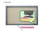
Page 98: ... 50XM3 29K00421 1 M50 INDICATOR 50XM3 29K00421 Caution For removal it comes off when it is pressed strongly from the rear side of the front panel For installation remove the separator before adhesion Caution For removal it comes off when it is pressed strongly from the rear side of the front panel For installation remove the separator before adhesion 10 FRONT PANEL 10 10 ...

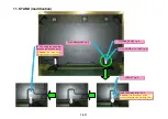
Page 99: ... CPIMS 4 12 15KF 1p 2 6 Fit it using the screw that has been removed as per 1 6 Fit it using the screw that has been removed as per 1 3 COVER POST 1p 2 3 COVER POST 1p 2 Caution The screw can be tightened only midway Caution The screw can be tightened only midway Caution Use a hexagon head wrench opposite side distance 5mm Caution Use a hexagon head wrench opposite side distance 5mm 11 STAND modif...

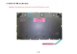
Page 100: ...VER modification 1 SRW32 CBIPS 4 12 15KFE 29N01401 12p 1 SRW32 CBIPS 4 12 15KFE 29N01401 12p Caution The illustration below shows a case when the STAND has been removed 2 FRONT PANEL ASSY 2 FRONT PANEL ASSY 10 12 ...

Page 101: ...ERMINAL PANEL M SUB ASSY 6 SRW17 TP M3 6 3KF 24N04581 4p 6 SRW17 TP M3 6 3KF 24N04581 4p 5 SRW25 TP M3 6 3KF 24N04581 3p 5 SRW25 TP M3 6 3KF 24N04581 3p 3 SRW17 TP M3 6 3KF 24N04581 3 SRW17 TP M3 6 3KF 24N04581 Caution It should be tightened together with the round terminal of the AD cable Caution It should be tightened together with the round terminal of the AD cable 4 CONNECTOR 12p 4 CONNECTOR 1...

Page 102: ...5 M27 SHIELD PLATE MAIN 42XM3 29H03541 5 M27 SHIELD PLATE MAIN 42XM3 29H03541 3 M52 TERMINAL SHEET M 50XM3 W 29K00571 3 M52 TERMINAL SHEET M 50XM3 W 29K00571 2 SRW15 CBIPS 3 8 3KF 24N03691 7p 2 SRW15 CBIPS 3 8 3KF 24N03691 7p 4 M28 TERMINAL PANEL M 50XM3 29H02551 4 M28 TERMINAL PANEL M 50XM3 29H02551 Caution After sticking the TERMINAL SHEET to the TERMINAL PANEL push the peripheral area of the sc...

Page 103: ... 6 3KF 24N04581 2 SRW26 TP M3 6 3KF 24N04581 5 M53 TERMINAL SHEET S 50XM3 W 29K00581 5 M53 TERMINAL SHEET S 50XM3 W 29K00581 Caution After sticking the TERMINAL SHEET to the TERMINAL PANEL push the peripheral area of the screw hole to strengthen the adhesion Caution After sticking the TERMINAL SHEET to the TERMINAL PANEL push the peripheral area of the screw hole to strengthen the adhesion Caution...

Page 104: ... M19 COVER SW 29F00721 2 M19 COVER SW 29F00721 3 M25 POWER BUTTON 50XM3 29G00281 3 M25 POWER BUTTON 50XM3 29G00281 4 A04 PWR PWB ASSY 937F7SC1 4 A04 PWR PWB ASSY 937F7SC1 Caution Positioning pin Use it in the case of reassembly Caution Positioning pin Use it in the case of reassembly Rear side 10 16 ...

Page 105: ...p 4 SRW27 TP M3 6 3KF 24N04581 3p 1 CONNECTOR 3p 1 CONNECTOR 3p 3 SRW23 TP M3 6 3KF 24N04581 2p 3 SRW23 TP M3 6 3KF 24N04581 2p M47 SILICONE SHEET AUDIO T 29J01291 M47 SILICONE SHEET AUDIO T 29J01291 Peel off the separator that is stuck to the rear side of the M71 AUDIO HEAT SINK 29H03561 Peel off the separator that is stuck to the rear side of the M71 AUDIO HEAT SINK 29H03561 10 17 ...

Page 106: ...B 61XM2 29K00551 9 M51 TERMINAL SHIEET B 61XM2 29K00551 3 M45 BARRIER INLET 29J01321 3 M45 BARRIER INLET 29J01321 Caution Mount it so that its bent side is positioned upwards Caution Mount it so that its bent side is positioned upwards 2 M17 INLET COLLAR 29F00481 2p 2 M17 INLET COLLAR 29F00481 2p Caution Insert it between the screw and the TERMINAL SHEET Caution Insert it between the screw and the...

Page 107: ...19 POWER UNIT 1 SRW14 PL CPIMS 4 12 15KFE 29N01441 6p 1 SRW14 PL CPIMS 4 12 15KFE 29N01441 6p 2 PSU POWER UNIT 3S110161 2 PSU POWER UNIT 3S110161 10 19 ...

Page 108: ...3 6 3KF 24N04581 1 SRW29 TP M3 6 3KF 24N04581 M44 BRACKET PC 29H03392 2p M44 BRACKET PC 29H03392 2p SRW36 PL CPIMS 4 12 15KFE 29N01441 4p SRW36 PL CPIMS 4 12 15KFE 29N01441 4p 8 E01 FAN MOTOR 9G1212M4D03 3S170014 2p 8 E01 FAN MOTOR 9G1212M4D03 3S170014 2p 7 SRW30 CFIMS3 30 15KFE 29N01481 6p 7 SRW30 CFIMS3 30 15KFE 29N01481 6p 9 E02 FAN MOTOR 9G1212M4D04 3S170015 9 E02 FAN MOTOR 9G1212M4D04 3S17001...

Page 109: ...Peripheral area of the BRACKET MAIN 3 SRW10 PL CPIMS 4 12 15KFE 29N01441 3p Peripheral area of the BRACKET FAN 3 SRW10 PL CPIMS 4 12 15KFE 29N01441 3p Peripheral area of the BRACKET FAN 5 SRW11 PL CPIMS 4 12 15KFE 29N01441 3p BRACKET SENSOR 5 SRW11 PL CPIMS 4 12 15KFE 29N01441 3p BRACKET SENSOR 4 SRW13 PL CPIMS 4 12 15KFE 29N01441 2p F BRACKET LR 4 SRW13 PL CPIMS 4 12 15KFE 29N01441 2p F BRACKET L...

Page 110: ... CLAMP M04 EDGING SADDLE EDS 1208U 29C00461 1p M05 CLAMP LCT 1S 29C00551 1p M64 CLAMP RLWC 2SV0 29C01901 34p M07 CLAMP RFCC 625 29C01721 1p M01 BUSHING INSULATOR 24282991 3p M09 CLAMP RBWS 5N 29C01741 2p 10 22 ...

Page 111: ...771 22p M11 GASKET L30 10 T10 29C01761 17p M11 GASKET L30 10 T10 29C01761 17p M13 GASKET L120 10 T10 29C01781 7p M13 GASKET L120 10 T10 29C01781 7p Caution Gaskets are used only for the CLASS B model PDP 614MX PRO 1410HD If replacement is intended the gasket should be carefully stuck without permitting it to protrude from the BACK COVER when this BACK COVER is being mounted 23 GASKET CLASS B 10 23...

Page 112: ...e back cover illustrated below Dimensions indicated are approximate figures However the presence of bends and air bubbles shall be reduced to a minimum Adhesion of the CCC label Stick the furnished CCC label approximately to the position indicated on the drawing of NAMEPLATE 61X 24 L LABELS ABELS 24L44791 29L03552 29L00491 Direction of adhesion 10 24 ...

Page 113: ...odule Wiring Diagram Front Block PX 61XM3J PX 61XM3A PX 61XM3W PS 61XR3A PX 61XR3W 25 WIRING LD SW Pass LD Pass SW x 7 Pass SW PARTS NAME PARTS NO Q TY EDGING SADDLE EDS 1208U 29C00461 2 CLAMP UAMS 05 2 29C01751 7 Exhaust pipe side AD Cable 10 25 ...

Page 114: ...t and the connector and confirm that there is no floating of parts x2 Pass TR and TS Pass TR TS and FC Pass TR and FC Pass TR FB and FC Pass TM and TR Pass PH Pass TR FB and FC Pass PH and PD Pass PD x2 Pass PD Pass TM FB and FC Pass TM FB and FC Pass TM FA FB and FC Pass FA and FB Pass PV PM PN and PA Pass GND and AC Pass GND and AC Pass AC Pass PV Pass 3 turns of GND Pass PW Pass RS Pass SW Pass...

Page 115: ...CORE ZCAT2032 930 6S170005 x 2pcs PK21 CORE FERRITE SFT 72SNB 6S170003 x 2pcs PX 61XM3A A BRACKET SASSY B ACCESSORY SASSY Put the EYEBOLTS MB 15KFE in the WARRANTY ENVELOPE 100 220 Then roll and fasten it with a tape Accommodated in the wrapped style BRACKET SASSY Fold it into an adequate size and fasten it with an adhesive tape Wire harness bandages x 2pcs Attached to the core METHOD OF PACKAGING...

Page 116: ...7S552001 Contained in the bagged state Front paper Align its direction and put it in SUPPLEMENT SHEET SUPPLEMENT SHEET SUPPLEMENT SHEET SUPPLEMENT SHEET Cables and others Accommodation layout diagram Seen from Arrow A Name Titled Circuit Symbol Material Name Material Code Quantity Needed Nil Nil Nil Nil Nil Nil Nil Nil Nil POWER CORD INFORMATION OPERATION NOTICE SHEET SUPPLEMENT SHEET INFORMATION ...

Page 117: ...he set Positioned so that the arrow mark faces the front plane of the set Positioned so that the arrow mark faces the front plane of the set Positioned so that the arrow mark faces the front plane of the set Positioned so that the arrow mark faces the front plane of the set To be folded inside 4 positions Positioned on the left as seen from the front so that the usage arrow mark face the front pla...

Page 118: ...ABLE 1P L400 7S530027 1 CN LD CN 5P LD 225 2468 26 7SU509LD 1 CN PA CN 6P PA 650 2468 26 7SU626PA 1 CN PD CN 10P PD 920W 1007 20 7SW0W010 1 CN PH CN 9P PH 360W 1007 20 7SW9W008 1 CN PI CN 2 WP PI 360W 1672 18 7SWXV002 1 CN PM CN 7P PM 450 2468 26 7SU718PM 1 CN PN CN 12P PN 475 2468 26 7SUB19PN 1 CN PV CN 8P PV 525 2468 26 7SU821PV 1 CN PW CN 8P PW 300 2468 26 7SC812PW 1 CN RS CN 12P RS 200 2468 26...

Page 119: ...5KFE 29N01441 6 SRW15 CBIPS 3 8 3KF 24N03691 7 SRW16 SCREW UNC4 40 4 40 32990229 4 SRW17 TP M3 6 3KF 24N04581 5 SRW18 NOT USED SRW19 SCREW UNC4 40 4 40 32990229 2 SRW20 TP M3 6 3KF 24N04581 1 SRW21 CBIPS 3 8 3KF 24N03691 2 SRW22 CPIMS NO 6 32UNC 8 3GF 29N01131 2 SRW23 TP M3 6 3KF 24N04581 2 SRW24 ET CBIMS 4 8 3KF 24N04001 1 SRW25 TP M3 6 3KF 24N04581 3 SRW26 TP M3 6 3KF 24N04581 1 SRW27 TP M3 6 3K...

Page 120: ...ET B OUT 29H02991 1 M38 BRACKET SENSOR 29H03001 1 M39 BRACKET MAIN 61XM3 29H03601 1 M40 SHIELD COVER MAIN 29H03021 1 M41 FAN BRACKET 29H03031 1 M42 TERMINAL PANEL B 61XM2 29H03191 1 M43 SHIELD CABLE 29H03231 1 M44 BRACKET PC 29H03392 2 M45 BARRIER INLET 29J01321 1 M46 NOT USED M47 SILICONE SHEET AUDIO T 29J01291 1 M48 CUSHION 782 10 T5 29J01171 2 M49 CUSHION 686 10 T5 29J01181 4 M50 INDICATOR 50XM...

Page 121: ...8 CUSHION BL 29MS2641 1 PK09 CUSHION BC 29MS2651 1 PK10 CUSHION BR 29MS2661 1 PK11 CUSHION BTM L 29MS2671 1 PK12 CUSHION BTM R 29MS2681 1 PK13 INNER CARTON 29MS2701 2 PK14 CARTON BOX T 61XM3 29MS3091 1 PK15 ACCESSORY BOX W 29MS1641 1 PK16 REM T HAND UNIT RP 114 3S120221 1 PK17 BAG POLYETHYLENE 150 370 24813191 1 PK18 CLAMP RST 1N 29C01511 5 PK19 FERRITE CORE ZCAT2032 930 6S170005 2 PK20 BATTERY DR...

Page 122: ...KG upper left Signal Relay PKG upper center Signal Relay PKG upper right Signal Relay PKG lower left Signal Relay PKG lower center Signal Relay PKG lower right Recovery Relay PKG 5 PKG61C2G3 02A 9S899671 1 6 PKG61C2E1 02B 9S899660 1 7 PKG61C2E2 02B 9S899661 1 8 PKG61C2J1 01B 9S899583 1 9 PKG61C2J2 01B 9S899584 1 10 PKG61C2J3 01B 9S899585 1 11 PKG61C2J4 01B 9S899586 1 12 PKG61C2J5 01B 9S899587 1 13...

Page 123: ...2 02C 18 22 03B 14 16 03C 24 28 04C 24 26 28 04D 26 28 05C 26 28 05D 26 28 Board ASSY interchangeability list in PDP NP61C2MF01 Note In the Board ASSY PKG replacement You can exchange it in a version of high rank than a replacement target version besides a compatible version Digital PKG follows the following list and exchange it Exchange it for 05C 27 9S899791 or 05D 27 9S899731 Exchange it for 05...

Page 124: ...12 A GND A 6 A 6 A GND A GND NC NC 1 2 3 4 1 2 3 4 1 2 3 4 TEMP SENSOR1 SENB PWB TEMP SENSOR2 SEND PWB TM SCL5 SDA5 VDD 5V GND SCL5 SDA5 VDD 5V GND SCL5 SDA5 VDD 5V GND 1 2 3 4 TR SCL5 SDA5 VDD 5V GND AU L GND AU R GND MUTE SCL7 SDA7 AU SHIELD WIRE 1 2 3 4 5 6 7 1 2 3 4 5 6 7 8 PW SW7 POIN GND M 5V M 7V REMIN1 LEDCTL1 LEDCTL2 1 2 3 29 30 31 AD PA AU 1 2 3 FAN CTL GND F ALM1 1 2 3 FAN CTL GND F ALM...

Page 125: ...put 0 Clock signal 3 3Vac when data are received 3 3Vdc when no data are received Clock signal 3 3Vac when data are received 3 3Vdc when no data are received Clock signal 3 3Vac when data are received 3 3Vdc when no data are received Clock signal 3 3Vac when data are received 3 3Vdc when no data are received 0 RS232C MAIN 5 M 3 3V 3 3V power supply for microcomputer 0 3 3 3 3 3 3 3 3 0 MAIN RS232C...

Page 126: ...V power supply for analog signals 0 3 3 3 3 0 0 0 SENB SEND 4 SDA5 Data line of the I2C bus 0 During data exchange Clock signal 3 3Vac Data not exchanged 3 3Vdc During data exchange Clock signal 3 3Vac Data not exchanged 3 3Vdc 0 0 0 SENB SEND TS 1 SCL5 Clock line of the I2C bus 0 Clock signal used during data transmission 3 3Vac 3 3Vdc when no data are transmitted Clock signal used during data tr...

Page 127: ...speed revolution Fan mode H 7 6Vdc during medium speed revolution Fan mode M 5 3Vdc during low speed revolution Fan mode L 9 3Vdc during high speed revolution Fan mode H 7 6Vdc during medium speed revolution Fan mode M 5 3Vdc during low speed revolution Fan mode L 0 0 0 2 GND GND 0 0 0 0 0 0 3 ALARM 42VM5 42VP5 42VR5 42XM3 42XR3 50XM4 50XR4 61XM3 61XR3 0 0V during normal fan operation 3 3V dc whil...

Page 128: ...LVDS serial differential G output 0 3Vac Bias 1 25Vdc OSD LVDS serial differential G output 0 3Vac Bias 1 25Vdc 0 0 0 MAIN PDP 13 RF Mode system output F 0 Video mode LVDS serial differential F output 0 3Vac Bias 1 25Vdc Video mode LVDS serial differential F output 0 3Vac Bias 1 25Vdc 0 0 0 MAIN PDP 14 RF Mode system output F 0 Video mode LVDS serial differential F output 0 3Vac Bias 1 25Vdc Video...

Page 129: ...ceived 5Vdc when no data are received Clock signal 5Vac when data are received 5Vdc when no data are received Clock signal 5Vac when data are received 5Vdc when no data are received Clock signal 5Vac when data are received 5Vdc when no data are received 0 LED PWR 2 LEDCTL1 Standby red LED control 0 0 0 3 3 3 3 0 PWR LED 3 LEDCTL2 POWER ON green LED control 0 3 3 3 3 0 0 0 PWR LED 4 GND GND 0 0 0 0...

Page 130: ... GND GND 0 0 0 0 0 0 3 D GND GND 0 0 0 0 0 0 4 D 5 5V power supply for digital circuits 0 5 15 5 15 0 0 0 POWER PDP 5 D GND GND 0 0 0 0 0 0 6 D GND GND 0 0 0 0 0 0 7 D 65 Vd power supply for PDP 0 65Vdc changeable according to the PDP 65Vdc changeable according to the PDP 0 0 0 POWER PDP 8 NC digital circuits 9 D 175 Vs power supply for PDP high voltage circuits 0 175Vdc changeable according to th...

Page 131: ...nverter Scaling correction Double pic processing TMDS Receiver CPU LVDS Transmitter To Module Analog signal line Digital signal line Control signal line VIDEO1 BNC VIDEO2 RCA VIDEO3 S DVD HD1 3RCA RGB2 DVD HD2 5BNC RGB1 D Sub RGB3 DVI Video SW for Loop Video SW for Loop γ PX 50XM4 61XM3 Series 15 1 BLOCK DIAGRAM ...

Page 132: ...ssing block I P converter Scaling correction Double pic processing TMDS Receiver CPU LVDS Transmitter To Module Analog signal line Digital signal line Control signal line VIDEO1 BNC VIDEO2 RCA VIDEO3 S DVD HD1 3RCA RGB2 DVD HD2 5BNC RGB1 D Sub RGB3 DVI γ PX 50XR4 61XR3 Series 15 2 BLOCK DIAGRAM ...

Reviews: