


PCM-072/phyCORE-AM64xx System on Module
L-860e.A0
© PHYTEC America L.L.C. 2022
44
6.2.2.1
MMC1 Pinout
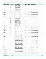
Table 15 MMC1 Connections at the phyCORE-Connector
X1 Pin #(s)
SOM Signal(s)
Type
Level Description
A30
X_MMC1_SDCD
(10K pullup)
I
3.3V
1
MMC1 Card Detection
A31
X_MMC1_SDWP
(10K pullup)
I
3.3V
1
MMC1 Write Protect
A13
X_MMC1_DAT3
I/O
3.3V
USDHC1 Data 3
A14
X_MMC1_DAT2
I/O
3.3V
USDHC1 Data 2
A16
X_MMC1_DAT1
I/O
3.3V
USDHC1 Data 1
A17
X_MMC1_DAT0
I/O
3.3V
USDHC1 Data 0
A11
X_MMC1_CLK
I/O
3.3V
USDHC1 Clock
A12
X_MMC1_CMD
I/O
3.3V
USDHC1 Command
1:
The voltage level for these signals is configurable between 1.8V and 3.3V. The default voltage level is listed here, but always check the actual jumper setting for the
applicable SOM configuration. Refer to
section
for details
6.2.2.2
MMC1 Design In Considerations
•
MMC1 signals should be length matched within 12700 µm as described in
•
Keep MMC1 trace lengths as short as possible.
•
Route the MMC1 clock with enough clearance from other signals, when possible, to reduce crosstalk. A general
rule is to use a clearance of at least 3 times the trace width.
•
It is r
ecommended to place series termination resistors (22Ω or similar is recommended) near the SD card on the
data and command signals.
•
SD card power should be connected to a 3.3V power supply regardless of the MMC1 IO voltage level.
•
SD card power needs to be toggled with on board power reset.
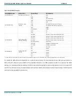
Table 16 phyCORE-AM64xx MMC1 Layout Characteristics
Signal Name
SOM Trace Length (µm)
Length Matching (µm)
Single Ended Impedance (Ω)
X_MMC1_DAT3
33087
12700
50
X_MMC1_DAT2
28616
X_MMC1_DAT1
33166
X_MMC1_DAT0
32396
X_MMC1_CLK
30210
X_MMC1_CMD
32302