EN 47
HTS5000W
9.
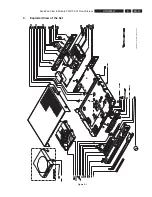
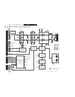
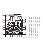
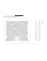
Exploded View & Module PWR 04-01 Non-Wireless
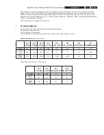
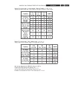
Dynamic DC measurements - currentconsuption / Mute and Standby.
( all values mA DC)
(
ampli
fi
erpcb loaded with 100 Ohm on F6 (3.3Vdc) and 50 Ohm on F5 (6VDC) // no audio input
Condition
Current
in +
27Vdc
Current
in -
27Vdc
Current
in +
6Vdc
LIMITS
F16 low
F10, F11 low
(Standby,
muted)
13
17
170
Typical
10
10
160
Lower
20
22
180
Higher
F16 to 3.3Vdc
F10, F11 low
(Amp on, but
muted)
80
84
173
Typical
72
75
171
Lower
87
90
175
Higher
F16 to 3.3Vdc
F10, F11 to
3.3Vdc
(Amp on,
demuted,
playmode)
88
80
172
Typical
80
75
170
Lower
100
95
175
Higher
Dynamic DC measurements / Serial communication
( all values Vdc)
The below table is valid if the 5Vdc supply is at its typical value of 5.4Vdc
Condition
F34
VOL_DAT
F33
VOL_CLOCK
F32
+5Vdc
LIMITS
F12 DATA
F14 CLOCK
To F13 Ground
with 330 ohms
series resistor
0.3
0.3
5.4
Typical
0
0
5.6
Lower
0.45
0.45
5.2
Higher
F12 DATA
F14 CLOCK
To F6 3.3 Vdc
5.3
5.3
5.4
Typical
5.1
5.1
5.6
Lower
5.5
5.5
5.2
Higher
Also read the datasheets of the M62429 for better understanding
For good serial communication to the Renesas chip:
The “low” level of Data and Clock should be max 0.2 x VCC
The “high” level of Data and Clock should be minimum 0.8 x VCC
(Re
fl
ected to our application: low level < 1.08 Vdc and high level > 4.3Vdc)
Summary of Contents for HTS5000W/12
Page 15: ...EN 15 HTS5000W FTD Display Pin Connection 6 6 FTD Display Pin Connection ...
Page 16: ...EN 16 HTS5000W Notes 6 FTD Display Pin Connection ...
Page 40: ...EN 40 HTS5000W Notes Circuit Diagram and PWB Layout 8 ...
Page 60: ...EN 60 HTS5000W 9 Exploded View Module PWR 04 01 Non Wireless Notes ...

