81
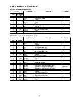
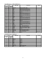
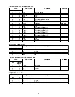
10 Explanation of Connector
CN3 [CONTROL Board] - SD Memory Card
Pin No.
Signal Name
Description
Remarks
CN3
SD Memory
Card
1
1
NSDCS
Chip Select Signal
Lower Active
2
2
SPIDO
Control Output Data
3
3
GND
Ground
4
4
+3.3VDD
+3.3 V
5
5
SPICLK
Clock
6
6
GND
Ground
7
7
SPIDI
Control Input Data
8
8
RSV
Reserve
9
9
RSV
Reserve
10
10
SPIEXIST
SD Card Detection Signal
11
11
Common
Ground
12
12
SPWP
Write Protect Signal
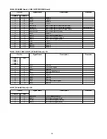
CN4 [CONTROL Board] - CN800 [MOTOR DRIVE Board]
Pin No.
Signal Name
Description
Remarks
CN4
CN800
1
1
+24 V
+ 24 V
2
2
+24 V
+ 24 V
3
3
PG
Ground
4
4
PG
Ground
5
5
INA
Motor Drive Signal (INA)
6
6
TDA
Motor Drive Signal (TDA)
7
7
INB
Motor Drive Signal (INB)
8
8
TDB
Motor Drive Signal (TDB)
9
9
AGND
Ground
10
10
AGND
Ground
11
11
PDOWN
Current Control Signal
12
12
RESERVE1
Reserved
13
13
+3.3AVDD
+ 3.3 V
14
14
+3.3AVDD
+ 3.3 V
15
15
+3.3AVDD
+ 3.3 V
16
16
HOME
Home Sensor Signal
17
17
RESERVE2
Reserved
18
18
AFESPDI
AFE Serial Signal (Control Input Signal)
19
19
NAFECS
AFE Serial Signal (Chip Select Signal)
Low Active
20
20
AFESPDO
AFE Serial Signal (Control Output Signal)
21
21
AFESPICLK
AFE Serial Signal (Clock)
22
22
AGND
Ground
23
23
RLED
LED Control Signal (Red)
24
24
GLED
LED Control Signal (Green)
25
25
BLED
LED Control Signal (Blue)
26
26
+5VCC
+ 5 V
27
27
AGND
Ground
28
28
+5VCC
+ 5 V
Summary of Contents for UB-5338C
Page 9: ...9 2 3 External View ...
Page 10: ...10 2 4 Control Panel Operation ...
Page 11: ...11 2 5 External Dimensions 2 5 1 UB 5838C ...
Page 12: ...12 2 5 2 UB 5338C ...
Page 101: ...101 13 Exploded View and Replacement Parts List ...
Page 102: ...102 13 1 Framework of Projected Diagram ...
Page 103: ...103 13 2 Cabinet Unit ...
Page 105: ...105 13 3 Motor Drive Unit Sensor Unit ...
Page 107: ...107 13 4 Control Box Unit ...
Page 109: ...109 13 5 Screen Feed Roller Unit ...
Page 111: ...111 13 6 Scanner Unit ...
Page 113: ...113 13 7 Panel Unit ...
Page 115: ...115 13 8 Frame Unit ...
Page 117: ...117 13 9 Rear Cover Unit ...
Page 119: ...119 13 10 Packing ...

