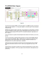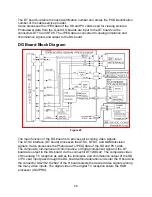
D Board Block Diagram
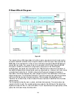
Figure 26
The output of the LVDS transmitter of the DG board is provided to the D board via the
connector DG5/D5. IC9500 of the D board contains a LVDS receiver that converts the
RGB data to its original form. In this IC, the customer and panel related OSD data are
mixed with the video. The output of the IC is provided to the Format Converter/RGB
Processor, IC9300, for interlace to progressive conversion of the 1080i signal.
Subsequently, all signals are converted to the 768P format to match the resolution of
the plasma display panel. Adjustments such as white balance, contrast, and color drives
are performed inside this IC. IC9300 contains the Plasma AI (Adaptive brightness
Intensifier) circuit that analyzes the video program level for the distribution of dark and
bright components. The Sub-field Processor is used to speed up the scanning process
and to control the number of sustain periods. This increases the brightness and
improves the contrast ratio. It also creates the two channels of data that drive the data
output boards.
The D-board provides the scan, sustain, and data drive signals. The scan pulses are
output to the SC board. The sustain pulses are output to the SS board. The data drive
signals are output to the C1, and C2 boards. The C1 board drives the right portion of the
panel; the C2 board drives the left portion.
32
Summary of Contents for TH-42PX50U
Page 40: ...SC board Waveform Figure 30 SU And SD Board Shift Registers Figure 31 35 ...
Page 43: ...SS Board Schematic Figure 33 SS Board Waveform Figure 34 38 ...
Page 66: ...Adjustment Volume Locations Figure 53 61 ...
Page 67: ...Test Point Locations Figure 54 62 ...
Page 71: ...Scan and Sustain Drive Waveform Figure 55 Scan and Sustain Drive Check points Figure 56 66 ...

