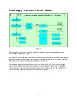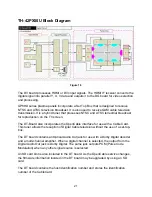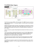
The DC voltage from the rectifier is converted to 395Vdc by the
“Power Factor
Control”
circuit to improve the power ratio.
This DC voltage is applied to three different circuits; the
Vsus
, the
Vda
and the
Low
Voltage
(F STB 14V, 15V, and 12V) power supplies.
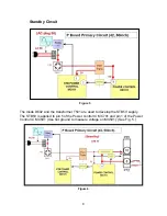
During standby operation, both the
Vsus
and the
Vda
power supply circuits are off.
Only the
“F STB 14V”
section of the
Low Voltage
power supply circuit is on.
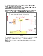
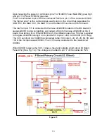
Figure 10
The
“F14V ON”
command (5V) from pin 10 of MC701 turns on Q452 and the
“F STB
14V”
is output to the PA-board through pins 1, 2, and 3 of connector P10.
(See Fig. 10)
Note:
The above description is true for standby mode only; the power has not been
turned on yet.
11
Summary of Contents for TH-42PX50U
Page 40: ...SC board Waveform Figure 30 SU And SD Board Shift Registers Figure 31 35 ...
Page 43: ...SS Board Schematic Figure 33 SS Board Waveform Figure 34 38 ...
Page 66: ...Adjustment Volume Locations Figure 53 61 ...
Page 67: ...Test Point Locations Figure 54 62 ...
Page 71: ...Scan and Sustain Drive Waveform Figure 55 Scan and Sustain Drive Check points Figure 56 66 ...

