Panasonic S-LINK V, Instruction Manual
The Panasonic S-LINK V user manual is essential for unlocking the full potential of this cutting-edge product. Easily download the comprehensive manual from our website, free of charge. Maximize your experience with the Panasonic S-LINK V by accessing step-by-step instructions and handy tips for seamless operation.
Share
Download


Reviews:
No comments
Related manuals for S-LINK V

RS500
Brand: Falcon Pages: 3

Securit 800L
Brand: C&K systems Pages: 2

6100 Series
Brand: Galcon Pages: 32

PSV5000
Brand: Data I/O Pages: 88

dap4 touch
Brand: Data Aire Pages: 13

UltraVoice
Brand: Federal Signal Corporation Pages: 60

VC-210
Brand: FASTRON. Pages: 16

sc200
Brand: Hach Pages: 2

ORBISPHERE 410
Brand: Hach Pages: 12

AS950 AWRS
Brand: Hach Pages: 472

sc1000
Brand: Hach Pages: 64

CL1
Brand: V2 ELETTRONICA Pages: 6

SC4500
Brand: Hach Pages: 210
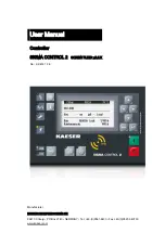
SIGMA CONTROL 2
Brand: KAESER KOMPRESSOREN Pages: 246

5980
Brand: Oceanic Systems Pages: 8

LB-ART2
Brand: LLURIA Pages: 2

BW3489
Brand: bihl+Wiedemann Pages: 16

NCSP35CM
Brand: IN-COMMAND Pages: 47


