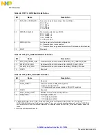
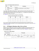


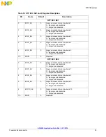


AN4536 Application Note Rev. 2.0 1/2014
32
Freescale Semiconductor
Hardware Considerations
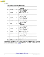
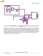
Figure 5. . Interfacing KITPFPGMEVME for application board MMPF0100 programming (Systems with
different VIN and VDDIO)
Note: Using the analog switch may not be the most cost effective option to supply VIN and VDDIO. Similar
functionality can be achieved by using solder shorts or 0 Ohm resistors. However, minor rework of the board would
be required once OTP programming is completed.
The Programmer_Select_O/P signal can be generated using the GPIO2 pin on the KITPFPGMEVME. Controlling
this signal can be part of the programming script.
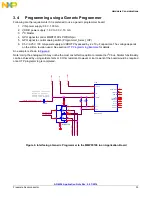
3.3V Regulator from KITPFPGMEVME
LDO REGULATOR 3.3V
R1
R2
3V3
3V3EN
INPUT
Program
m
e
r_Selec
t_O
/P
SYSTEM_VDDIO_SUPPLY
3V3
0
0
0
0
C88
470PF
MMPF0100/Z
U12A
ICTEST
5
INTB
1
RESETBMCU
3
SCL
54
SDA
53
SDWNB
2
STANDBY
4
VCOREDIG
51
VCOREREF
52
VDDIO
55
VDDOTP
47
PWRON
56
VCORE
49
GNDREF
48
VIN
50
R88
12.0K
U13
NC7SB3157L6X
B1
1
GND
2
B0
3
A
4
VCC
5
S
6
+
C91
2.2UF
C90
1.0UF
R91
4.7K
C89
2.2uF
DNP
U11
MIC5205
IN
1
GND
2
ADJ
4
EN
3
OUT
5
R87
20K
R90
4.7K