


AN4536 Application Note Rev. 2.0 1/2014
Freescale Semiconductor
15
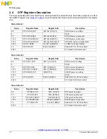
OTP Overview
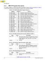
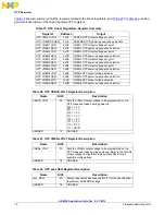
Table 16. OTP SWx CONFIG Register Description
Name
Bit #
Description
SWx_FREQ
1:0
SWx OTP Frequency configuration
00 = 1.0 MHz
01 = 2.0 MHz
10 = 4.0 MHz
11 = Reserved
SWx_CONFIG
3:2
SWx configuration
(3)
SW1A/B
00 = A/B/C Single Phase
01 = A/B Single Phase - C
Independent
10 = A/B Dual Phase - C
Independent
11 = Reserved
SW3A
00 = A/B Single Phase
01 = A/B Single Phase
10 = A/B Dual Phase
11 = A/B Independent
mode
VTT
4
Enable SW4 in VTT mode
(4)
UNUSED
7:5
UNUSED
Notes
3. Only on OTP SW1AB CONFIG and OTP SW3A CONFIG registers. UNUSED on all other OTP SWx
CONFIG registers.
4. Only on OTP SW4 CONFIG register. UNUSED on all other OTP SWx CONFIG registers.
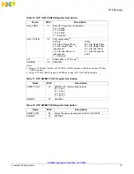
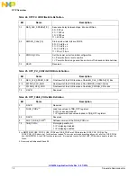
Table 17. OTP SWBST VOLT Register Description
Name
Bit #
Description
SWBST_VOLT
1:0
SWBST OTP output voltage setpoint
00 = 5.00 V
01 = 5.05 V
10 = 5.10 V
11 = 5.15 V
UNUSED
7:2
UNUSED
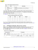
Table 18. OTP SWBST SEQ Register Description
Name
Bit #
Description
SWBST_SEQ
4:0
Assign the power-up sequence slot 0-31 for SWBST
UNUSED
7:5
UNUSED