


AN4536 Application Note Rev. 2.0 1/2014
26
Freescale Semiconductor
OTP Overview
2.5.2.3
Fuse Programming with ECC
To program fuses with ECC, bits in the following registers must be enabled:
•
OTP EN ECC0 and OTP EN ECC1 in the Extended Page 1
•
OTP AUTO ECC0 and OTP AUTO ECC1 in the Extended Page 2.
The ECC enable registers are shown in
Table 38
. Enable error correction for any bank by setting the appropriate
bit. Bits in the OTP EN ECCx registers are programmed and not just set in software.
The OTP AUTO ECC registers are shown in
Table 39
. After the fuses are programmed, their values may be loaded
to the TBBOTP registers. The values loaded are the error-corrected values if there was a single bit error in any bank.
To view the uncorrected or raw fuse values see the
Direct OTP Fuse Read
section. To determine if there was an
error when programming fuses, the following options are available:
•
Checking the fuse values against what was written.
•
Monitor the INTB signal, but first the ECC interrupt must be unmasked.
•
Read bits[5:0] from the OTP ECC CTRLx registers in the Extended Page 2. See
Table 37
to decipher single
bit error codes and
Table 41
for a description of the ECC registers.
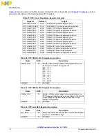
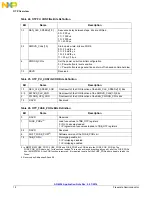
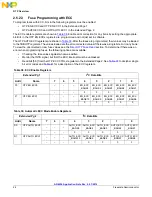
Table 38. ECC Enable Registers
Extended Pg 1
I
2
C Data Bits
Addr
Name
7
6
5
4
3
2
1
0
F0
OTP EN ECC0
–
–
–
EN_ECC
_BANK5
EN_ECC
_BANK4
EN_ECC
_BANK3
EN_ECC
_BANK2
EN_ECC
_BANK1
–
–
–
0
0
0
0
0
F1
OTP EN ECC1
–
–
–
EN_ECC
_BANK10
EN_ECC
_BANK9
EN_ECC
_BANK8
EN_ECC
_BANK7
EN_ECC
_BANK6
–
–
–
0
0
0
0
0
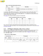
Table 39. Automatic ECC Mode Enable Registers
Extended Pg 2
I
2
C Data Bits
Addr Name
7
6
5
4
3
2
1
0
D0
OTP AUTO ECC0
–
–
–
AUTO_ECC
_BANK5
AUTO_ECC
_BANK4
AUTO_ECC
_BANK3
AUTO_ECC
_BANK2
AUTO_ECC
_BANK1
–
–
–
0
0
0
0
0
D1
OTP AUTO ECC1
–
–
–
AUTO_ECC
_BANK10
AUTO_ECC
_BANK9
AUTO_ECC
_BANK8
AUTO_ECC
_BANK7
AUTO_ECC
_BANK6
–
–
–
0
0
0
0
0