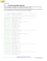


AN4536 Application Note Rev. 2.0 1/2014
22
Freescale Semiconductor
OTP Overview
2.5.2
Error Correction Code (ECC)
Error correction is off by default, but it is recommended for all OTP programming operations. When enabled, it
reports and corrects a single bit error per fuse bank, but only reports a double bit error per fuse bank. Fuses may be
programmed without using ECC. However, after verifying that the part is configured properly, ECC may enabled,
and the error check bits can be programmed.
It should be noted that double bit errors can prevent regulators from powering up, or can result in a configuration
that does not match the external components. Although such occurrence is rare, it is still a good practice to employ
ECC to at least alert the user of such an occurrence.
Note: The desired function of the redundant bits must be determined when ECC is configured and its bits
programmed, or the ECC logic attempts to correct the newly programmed redundant bits.
Sections
2.5.2.1
through
2.5.2.3
are for advanced users. For a simple script that enables ECC, proceed to section
OTP Programming Example
.
2.5.2.1
ECC Interrupt
With ECC enabled, if a single fuse in a bank has the wrong value, the ECC logic corrects that bit and the corrected
value is loaded into the TBBOTP register for that bank. The single error bit for that bank is set and also the main
interrupt ECC bit is set. If two or more bits are in error, in a bank, the ECC is not able to correct them. The double
error bit error for that bank is set and the ECC interrupt bit is set. The single error and double error bits may be read
from registers 0x8A to 0x8D in the Extended Page1 of the register map. The ECC interrupt bit may be read from
register, 0xE, on the functional page of the register map.
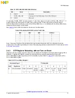
Table 34. ECC Error Detection Registers
Extended Page 1
I
2
C Data Bits
Addr
Reg Name
7
6
5
4
3
2
1
0
8A
OTP ECC SE1
–
–
–
ECC5_SE ECC4_SE ECC3_SE ECC2_SE ECC1_SE
x
x
x
0
0
0
0
0
8B
OTP ECC SE2
–
–
–
ECC10_SE ECC9_SE ECC8_SE ECC7_SE ECC6_SE
x
x
x
0
0
0
0
0
8C
OTP ECC DE1
–
–
–
ECC5_DE ECC4_DE ECC3_DE ECC2_DE ECC1_DE
x
x
x
0
0
0
0
0
8D
OTP ECC DE2
–
–
–
ECC10_DE ECC9_DE ECC8_DE ECC7_DE ECC6_DE
x
x
x
0
0
0
0
0