


AN4536 Application Note Rev. 2.0 1/2014
10
Freescale Semiconductor
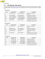
OTP Overview
2.4
OTP Registers Description
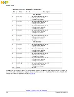
There are ten banks with a total of 260 fuses, where each bank contains 26 fuses. Each fuse represents one bit of
the TBBOTP register map.
Table 2
to
Table 11
show the banks, their fuses and the corresponding bits in the register
map.
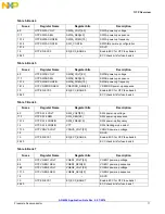
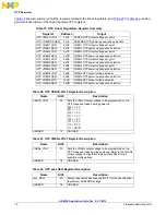
Table 2. Bank 1
Fuses
Register Name
Register bits
Description
5:0
OTP SW1AB VOLT
SW1AB_VOLT[5:0]
SW1AB power-up voltage
6
–
–
RSVD
11:7
OTP SW1AB SEQ
SW1AB_SEQ[4:0]
SW1AB power-up sequence
13:12
OTP SW1AB CONFIG
SW1AB_FREQ[1:0]
SW1AB power-up frequency
15:14
OTP SW1AB CONFIG
SW1AB_CONFIG[1:0]
SW1A/B/C power-up configuration
18:16
OTP I2C ADDR
I2C_SLV_ADDR[3:0]
3 LSBs of the slave address
19
OTP EN ECC0
EN_ECC_BANK1
Enable ECC for OTP fuse bank 1
25:20
–
–
ECC check bits for fuse bank 1
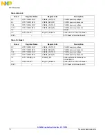
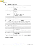
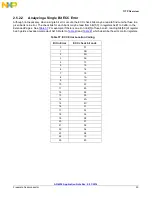
Table 3. Bank 2
Fuses
Register Name
Register bits
Description
5:0
OTP SW1C VOLT
SW1C_VOLT[5:0]
SW1C power-up voltage
6
–
–
RSVD
11:7
OTP SW1C SEQ
SW1C_SEQ[4:0]
SW1C power-up sequence
13:12
OTP SW1C CONFIG
SW1C_FREQ[1:0]
SW1C power-up frequency
15:14
OTP SWBST VOLT
SWBST[1:0]
SWBST power-up voltage
18:16
–
–
RSVD
19
OTP EN ECC0
EN_ECC_BANK2
Enable ECC for OTP fuse bank 2
25:20
–
–
ECC check bits for fuse bank 2
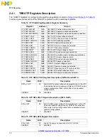
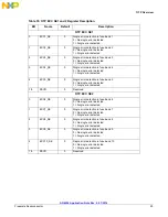
Table 4. Bank 3
Fuses
Register Name
Register bits
Description
6:0
OTP SW2 VOLT
SW2_VOLT6:0]
SW2 power-up voltage
11:7
OTP SW2 SEQ
SW2_SEQ[4:0]
SW2 power-up sequence
13:12
OTP SW2 CONFIG
SW2_FREQ[1:0]
SW2 power-up frequency
18:14
OTP SWBST SEQ
SWBST_SEQ[4:0]
SWBST power-up sequence
19
OTP EN ECC0
EN_ECC_BANK3
Enable ECC for OTP fuse bank 3
25:20
–
–
ECC check bits for fuse bank 3