


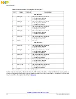


AN4536 Application Note Rev. 2.0 1/2014
30
Freescale Semiconductor
Hardware Considerations
3.3
Programming using the PF-Programmer
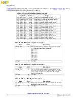
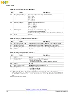
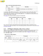
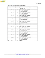
The KITPFPGMEVME is Freescale's programming board that can be used to OTP program the MMPF0100. It
integrates a 3.3 V LDO to power the MMPF0100 and a boost converter with an adjustable output voltage to generate
the OTP programming voltage. An integrated USB-to-I
2
C converter allows PC communication with the MMPF0100
using a Freescale supplied GUI. See
Figure 3
for a block diagram of KITPFPGMEVME.
Figure 3. KITPFPGMEVME Block Diagram
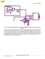
The V3V3 rail generates a 3.3 V supply to power the VIN and VDDIO rails of the MMPF0100.
Figure 4
shows how
to interface the KITPFPGMEVME with the MMPF0100 in an application board. For applications which use a single
rail for VIN and VDDIO, the connection is straightforward as shown in
Figure 4
. However, it must be ensured that
other loads connected to the 3.3 V rail do not surpass the current rating of the LDO. If that is the case, isolation in
the form of an analog switch, a solder short, or a 0 Ohm resistor is required.
VPGM
V3V3
GND
SDA
SCL
PWRON
VUSB
ID
D+
D-
GND
1
2
3
4
5
PROGRAMMING
INTERFACE
6
1
2
3
4
5
MINI-USB
INTERFACE
BOOST
LDO
MCU
+3.3V
+8.25V
+3.5V to 5.5V
VIN
BSTEN
GND
VOUT
GND
GND
VIN
VOUT
SHDN
PGMEN
D-
SCL
SDA
PWRON
VDD
D+
CONNECTED
PROGON
3V3EN
VINSNS
EN
FB
VUSBEN
S1
S2
UP
DN
BSTDN
BSTUP
DACOUT
7
8
GPIO1
GPIO2
GPIO1
GPIO2