


AN4536 Application Note Rev. 2.0 1/2014
14
Freescale Semiconductor
OTP Overview
2.4.1
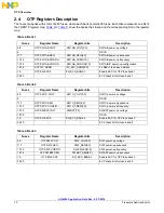
TBBOTP Registers Description
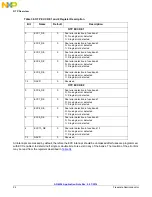
The TBBOTP registers for configuring the switching regulators are listed in
Table 12
and
Table 13
to
Table 18
provide a general description of the TBBOTP registers for all the switching regulators.
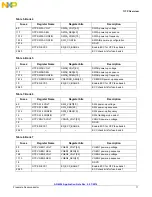
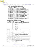
Table 12. OTP Switching Regulators Register Summary
Register Address
Output
OTP SW1AB VOLT
0xA0
SW1AB OTP Output voltage set point
OTP SW1AB SEQ
0xA1
SW1AB OTP power-up sequence selection
OTP SW1AB CONFIG
0xA2
SW1AB OTP operation mode and frequency selection
OTP SW1C VOLT
0xA8
SW1C OTP Output voltage set point
OTP SW1C SEQ
0xA9
SW1C OTP power-up sequence selection
OTP SW1C CONFIG
0xAA
SW1C OTP frequency selection
OTP SW2 VOLT
0xAC
SW2 OTP Output voltage set point
OTP SW2 SEQ
0xAD
SW2 OTP power-up sequence selection
OTP SW2 CONFIG
0xAE
SW2 OTP frequency selection
OTP SW3AVOLT
0xB0
SW3A OTP Output voltage set point
OTP SW3A SEQ
0xB1
SW3A OTP power-up sequence selection
OTP SW3A CONFIG
0xB2
SW3A OTP operation mode and frequency selection
OTP SW3B VOLT
0xB4
SW3B OTP Output voltage set point
OTP SW3B SEQ
0xB5
SW3B OTP power-up sequence selection
OTP SW3B CONFIG
0xB6
SW3B OTP frequency selection
OTP SW4 VOLT
0xB8
SW4 OTP output voltage set point
OTP SW4 SEQ
0xB9
SW4 OTP power-up sequence selection
OTP SW4 CONFIG
0xBA
SW4 OTP frequency and VTT mode selection
OTP SWBST VOLT
0xBC
SWBST OTP output voltage set point
OTP SWBST SEQ
0xBD
SWBST OTP power-up sequence selection
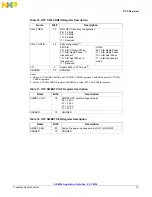
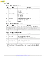
Table 13. OTP SW1x VOLT Register Description (SW1A/B and SW1C)
Name
Bit #
Description
SW1x_VOLT
5:0
Sets the SW1x output voltage to be programmed on the OTP
fuses and loaded during power-up. Refer to SW1A/B/C output
voltage configuration table on Data Sheet for all possible
configurations.
UNUSED
7:6
UNUSED
Table 14. OTP SWx VOLT Register Description (SW2 - SW4)
Name
Bit #
Description
SWx_VOLT
6:0
Sets the SWx output voltage to be programmed on the OTP
fuses and loaded during power-up. Refer to the respective
SWx output voltage configuration table on datasheet for all
possible configurations.
UNUSED
7
UNUSED
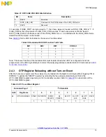
Table 15. OTP SWx SEQ Register Description
Name
Bit #
Description
SWx_SEQ
4:0
Assign the power-up sequence slot 0-31 for SWx
UNUSED
7:5
UNUSED