background image

254

APPENDIX A   DEVELOPMENT TOOLS

User’s Manual  U15104EJ2V0UD

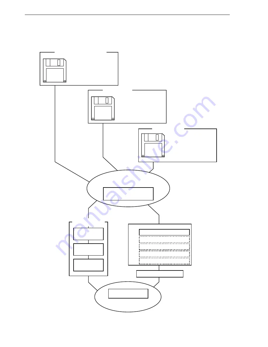
Figure A-1.  Configuration of Development Tools (2/2)

(2) When using the in-circuit emulator IE-78001-R-A

Remark

Items in broken line boxes differ according to the development environment.  Refer to A.5  Debugging

Tools (Hardware).

• System simulator
• Integrated debugger
• Device file

Embedded Software

• Real-time OS
• OS

Debugging Tool

• Assembler package
• C compiler package
• C library source file
• Device file

Language Processing Software

Flash memory 
write adapter

In-Circuit Emulator

Emulation probe

Conversion socket or 
conversion adapter

Target system

Host Machine (PC or EWS)

Interface board 

Interface adapter

Emulation board

I/O board

Probe board

Emulation probe conversion board

On-chip flash 
memory version

Flash Memory 

Write Environment

Flash programmer

Summary of Contents for mPD178053

Page 1: ...User s Manual Printed in Japan µPD178054 Subseries 8 Bit Single Chip Microcontrollers µPD178053 µPD178054 µPD178F054 Document No U15104EJ2V0UD00 2nd edition Date Published January 2002 N CP K 2001 ...

Page 2: ...2 User s Manual U15104EJ2V0UD MEMO ...

Page 3: ... devices must be fixed high or low by using a pull up or pull down circuitry Each unused pin should be connected to VDD or GND with a resistor if it is considered to have a possibility of being an output pin All handling related to the unused pins must be judged device by device and related specifications governing the devices 3 STATUS BEFORE INITIALIZATION OF MOS DEVICES Note Power on does not ne...

Page 4: ...ising from the use of these circuits software and information While NEC endeavours to enhance the quality reliability and safety of NEC semiconductor products customers agree and acknowledge that the possibility of defects thereof cannot be eliminated entirely To minimize risks of damage to property or injury including death to persons arising from defects in NEC semiconductor products customers m...

Page 5: ...C Electronics Germany GmbH Duesseldorf Germany Tel 0211 65 03 02 Fax 0211 65 03 490 NEC Electronics UK Ltd Milton Keynes UK Tel 01908 691 133 Fax 01908 670 290 NEC Electronics Italiana s r l Milano Italy Tel 02 66 75 41 Fax 02 66 75 42 99 NEC Electronics Germany GmbH Benelux Office Eindhoven The Netherlands Tel 040 2445845 Fax 040 2444580 NEC Electronics France S A Velizy Villacoublay France Tel 0...

Page 6: ...g Alternate Functions p 124 Modification of description in 3 Oscillation stabilization time select register OSTS in 8 3 Registers Controlling Watchdog Timer p 240 Addition of CHAPTER 19 ELECTRICAL SPECIFICATIONS p 250 Addition of CHAPTER 20 PACKAGE DRAWING p 251 Addition of CHAPTER 21 RECOMMENDED SOLDERING CONDITIONS p 253 Modification of Figure A 1 Configuration of Development Tools pp 255 256 Ad...

Page 7: ...of electric and logic circuits and microcomputers When you want to understand the functions in general Read this manual in the order of the contents To know the µPD178054 Subseries instruction function in detail Refer to the 78K 0 Series User s Manual Instructions U12326E How to interpret the register format For the circled bit number the bit name is defined as a reserved word in DF178054 and RA78...

Page 8: ...sembly Language U14446E Structured Assembly Language U11789E CC78K0 C Compiler Operation U14297E Language U14298E SM78K0S SM78K0 System Simulator Ver 2 10 or Later Operation U14611E Windows Based SM78K Series System Simulator Ver 2 10 or Later External Part User Open U15006E Interface Specifications ID78K0 NS Integrated Debugger Ver 2 00 or Later Operation U14379E Windows Based ID78K0 Integrated D...

Page 9: ...mer User s Manual U13502E Other Related Documents Document Name Document No SEMICONDUCTOR SELECTION GUIDE Products Packages X13769E Semiconductor Device Mounting Technology Manual C10535E Quality Grades on NEC Semiconductor Devices C11531E NEC Semiconductor Device Reliability Quality Control System C10983E Guide to Prevent Damage for Semiconductor Devices by Electrostatic Discharge ESD C11892E Cau...

Page 10: ... 2 6 P60 to P67 Port 6 31 2 2 7 P70 to P77 Port 7 31 2 2 8 P120 to P125 Port 12 32 2 2 9 P130 to P132 Port 13 32 2 2 10 EO0 EO1 32 2 2 11 VCOL VCOH 32 2 2 12 AMIFC 33 2 2 13 FMIFC 33 2 2 14 RESET 33 2 2 15 X1 X2 33 2 2 16 REGOSC 33 2 2 17 REGCPU 33 2 2 18 VDD 33 2 2 19 GND 33 2 2 20 VDDPORT 33 2 2 21 GNDPORT 33 2 2 22 VDDPLL 33 2 2 23 GNDPLL 33 2 2 24 VPP µPD178F054 only 33 2 2 25 IC Mask ROM vers...

Page 11: ...sing 67 3 4 9 Stack addressing 67 CHAPTER 4 PORT FUNCTIONS 68 4 1 Port Functions 68 4 2 Port Configuration 70 4 2 1 Port 0 70 4 2 2 Port 1 71 4 2 3 Port 3 72 4 2 4 Port 4 74 4 2 5 Port 5 75 4 2 6 Port 6 76 4 2 7 Port 7 77 4 2 8 Port 12 80 4 2 9 Port 13 82 4 3 Registers Controlling Port Functions 83 4 4 Port Function Operations 87 4 4 1 Writing to I O ports 87 4 4 2 Reading from I O ports 87 4 4 3 ...

Page 12: ...lling Watchdog Timer 121 8 4 Operations of Watchdog Timer 125 8 4 1 Watchdog timer operation 125 8 4 2 Interval timer operation 126 CHAPTER 9 BUZZER OUTPUT CONTROLLER 127 9 1 Functions of Buzzer Output Controllers 127 9 2 Configuration of Buzzer Output Controllers 128 9 3 Registers Controlling Buzzer Output Controllers 128 9 3 1 BEEP0 128 9 3 2 BUZ 129 9 4 Operation of Buzzer Output Controllers 12...

Page 13: ...of PLL frequency synthesizer 189 13 5 PLL Disable Status 194 13 6 Notes on PLL Frequency Synthesizer 194 CHAPTER 14 FREQUENCY COUNTER 195 14 1 Function of Frequency Counter 195 14 2 Configuration of Frequency Counter 195 14 3 Registers Controlling Frequency Counter 197 14 4 Operation of Frequency Counter 199 14 5 Notes on Frequency Counter 201 CHAPTER 15 STANDBY FUNCTION 203 15 1 Standby Function ...

Page 14: ...0 CHAPTER 20 PACKAGE DRAWING 250 CHAPTER 21 RECOMMENDED SOLDERING CONDITIONS 251 APPENDIX A DEVELOPMENT TOOLS 252 A 1 Software Package 255 A 2 Language Processing Software 255 A 3 Control Software 256 A 4 Flash Memory Writing Tools 256 A 5 Debugging Tools Hardware 257 A 6 Debugging Tools Software 259 A 7 Embedded Software 260 A 8 System Upgrade from Former In circuit Emulator for 78K 0 Series to I...

Page 15: ...5 Block Diagram of P30 to P32 and P35 72 4 6 Block Diagram of P33 and P34 73 4 7 Block Diagram of P36 and P37 73 4 8 Block Diagram of P40 to P47 74 4 9 Block Diagram of Key Input Detector 75 4 10 Block Diagram of P50 to P57 75 4 11 Block Diagram of P60 to P67 76 4 12 Block Diagram of P70 P74 and P77 77 4 13 Block Diagram of P71 and P75 78 4 14 Block Diagram of P72 and P76 78 4 15 Block Diagram of ...

Page 16: ...Timer Count Operation 116 7 1 Block Diagram of Basic Timer 117 7 2 Operation Timing of Basic Timer 118 7 3 Operating Timing to Poll BTMIF0 Flag 118 8 1 Block Diagram of Watchdog Timer 119 8 2 Format of Watchdog Timer Clock Select Register WDCS 122 8 3 Format of Watchdog Timer Mode Register WDTM 123 8 4 Format of Oscillation Stabilization Time Select Register OSTS 124 9 1 Block Diagram of BEEP0 127...

Page 17: ...12 10 Interrupt Request Acknowledgement Processing Algorithm 170 12 11 Interrupt Request Acknowledgement Timing Minimum Time 171 12 12 Interrupt Request Acknowledgement Timing Maximum Time 171 12 13 Multiple Interrupt Servicing Example 174 12 14 Pending Interrupt Request 176 13 1 Block Diagram of PLL Frequency Synthesizer 179 13 2 Format of PLL Mode Select Register PLLMD 181 13 3 Format of PLL Ref...

Page 18: ...T Input 213 16 3 Timing of Reset due to Watchdog Timer Overflow 214 16 4 Timing of Reset by Power on Clear 215 16 5 Format of POC Status Register POCS 218 16 6 Format of POC Status Register POCS 219 17 1 Format of Memory Size Switching Register IMS 221 17 2 Format of Internal Expansion RAM Size Switching Register IXS 222 17 3 Format of Communication Mode Selection 223 17 4 Connection of Flashpro I...

Page 19: ...nadvertent Program Loop Detection Time 125 8 5 Interval Timer Interval Time 126 9 1 Configuration of Buzzer Output Controllers 128 10 1 Configuration of A D Converter 130 11 1 Configuration of Serial Interfaces SIO30 to SIO32 149 12 1 Interrupt Sources 157 12 2 Various Flags Corresponding to Interrupt Request Sources 160 12 3 Times from Maskable Interrupt Request Generation to Interrupt Servicing ...

Page 20: ...hing Register 221 17 3 Set Value of Internal Expansion RAM Size Switching Register 222 17 4 Communication Modes 223 17 5 Major Functions of Flash Memory Programming 224 17 6 Setting Example for Flashpro III PG FP3 225 18 1 Operand Symbols and Descriptions 227 21 1 Surface Mounting Type Soldering Conditions 251 A 1 System Upgrade Method from Former In circuit Emulator for 78K 0 Series to IE 78001 R...

Page 21: ...face 3 channels 3 wire serial I O mode 2 channels 3 wire serial I O mode on chip time division transfer function 1 channel Timer 6 channels Basic timer timer carry FF 1 channel 8 bit timer event counter 4 channels Watchdog timer 1 channel Buzzer output Vectored interrupt Item Non Maskable Maskable InterruptNote Software Interrupt Part Number InterruptNote External Internal µPD178053 178054 178F054...

Page 22: ...04EJ2V0UD 1 2 Applications Car stereos 1 3 Ordering Information Part Number Package µPD178053GC 8BT 80 pin plastic QFP 14 14 µPD178054GC 8BT 80 pin plastic QFP 14 14 µPD178F054GC 8BT 80 pin plastic QFP 14 14 Remark indicates ROM code suffix ...

Page 23: ...P15 ANI5 P70 SI30 P71 SO30 P72 SCK30 P73 P74 SI31 P75 SO31 P76 SCK31 P77 TI52 P130 TO50 P131 TO51 P132 TO52 P40 P41 P42 1 2 3 4 5 6 7 8 9 10 11 12 13 14 15 16 17 18 19 20 P37 BUZ P36 BEEP0 P35 P34 TI51 P33 TI50 P32 P31 P30 P67 P66 P65 P64 P63 P62 P61 P60 P57 P56 P55 P54 60 59 58 57 56 55 54 53 52 51 50 49 48 47 46 45 44 43 42 41 RESET V DD REGOSC X1 X2 GND REGCPU P06 P05 P04 INTP4 P03 INTP3 P02 IN...

Page 24: ... P47 Port 4 P50 to P57 Port 5 P60 to P67 Port 6 P70 to P77 Port 7 P120 to P125 Port 12 P130 to P132 Port 13 REGCPU Regulator for CPU power supply REGOSC Regulator for oscillator RESET Reset input SCK30 SCK31 Serial SIO3 clock input output SCK32 SCK321 SI30 SI31 SI32 Serial SIO3 data input SI321 SO30 SO31 Serial SIO3 data output SO32 SO321 TI50 to TI52 8 bit timer clock input TO50 to TO52 8 bit tim...

Page 25: ... µ PD178F054 Enhanced timer 3 wire serial I O 80 pins 80 pins PD178054 Subseries µ µ PD178F124 On chip IEBus controller 80 pins 80 pins PD178024 Subseries µ µ On chip IEBusTM controller UART Enhanced timer 3 wire serial I O On chip UART PD178F048 On chip OSD controller 8 bit PWM 4 channels 14 bit PWM 1 channel 80 pins 80 pins PD178048 Subseries µ µ On chip OSD controller 8 bit PWM 4 channels 14 bi...

Page 26: ...ency counter PLL voltage regulator Buzzer output 78K 0 CPU Core RAM 1024 bytes ROM Flash memory TI50 P33 TO50 P130 P00 to P06 P10 to P15 P30 to P37 P40 to P47 P50 to P57 P60 to P67 P70 to P77 P120 to P125 P130 to P132 ANI0 P10 to ANI5 P15 AMIFC FMIFC EO0 EO1 VCOL VCOH VDDPLL GNDPL IC Vpp L SI30 P70 SO30 P71 SCK30 P72 Serial interface31 SI31 P74 SO31 P75 SCK31 P76 SI32 P120 SO32 P121 SCK32 P122 SI3...

Page 27: ...counter 4 channels Watchdog timer 1 channel Buzzer output BEEP pin 1 kHz 1 5 kHz 3 kHz 4 kHz BUZ pin 549 Hz 1 10 kHz 2 20 kHz 4 39 kHz Vectored Maskable Internal 11 interrupt External 5 sources Non maskable Internal 1 Software 1 PLL Division mode 2 types frequency Direct division mode VCOL pin synthesizer Pulse swallow mode VCOL and VCOH pins Reference frequency Seven types selectable in software ...

Page 28: ...fied in 1 bit units An on chip pull up resistor can be specified by software Interrupt function by key input is provided P50 to P57 I O Port 5 Input 8 bit I O port Input output can be specified in 1 bit units P60 to P67 I O Port 6 Input 8 bit I O port Input output can be specified in 1 bit units P70 I O Port 7 Input SI30 P71 8 bit I O port SO30 P72 Input output can be specified in 1 bit units SCK3...

Page 29: ...tput Input P36 BUZ P37 ANI0 to ANI5 Input Analog input to A D converter Input P10 to P15 EO0 EO1 Output Error out output from charge pump of PLL frequency synthesizer VCOL Input Inputs local oscillation frequency of PLL in HF and MF modes VCOH Inputs local oscillation frequency of PLL in VHF mode AMIFC Input Input to AM intermediate frequency counter Input FMIFC Input to FM or AM intermediate freq...

Page 30: ...0 to P15 constitute a 6 bit input port In addition to input port pins P10 to P15 function as A D converter analog inputs The following operating modes can be specified in 1 bit units 1 Port mode These pins function as a 6 bit input port 2 Control mode These pins function as A D converter analog input pins ANI0 to ANI5 2 2 3 P30 to P37 Port 3 P30 to P37 constitute an 8 bit I O port In addition to I...

Page 31: ... port These pins can be specified as input or output in 1 bit units using port mode register 6 PM6 2 2 7 P70 to P77 Port 7 P70 to P77 pins constitute an 8 bit I O port In addition to port pins P70 to P77 also function as serial interface data I O clock I O and a timer input The following operating modes can be specified in 1 bit units 1 Port mode These pins function as an 8 bit I O port for which ...

Page 32: ...n 1 bit units 1 Port mode These pins function as a 3 bit output port 2 Control mode These pins function as output pins for the 8 bit timer event counter TO50 TO51 TO52 These pins are output pins for the 8 bit timer event counter 2 2 10 EO0 EO1 These are the output pins of the charge pump of the PLL frequency synthesizer They output the result of phase comparison between the frequency divided by th...

Page 33: ...y counter 2 2 14 RESET Low level active system reset input pin 2 2 15 X1 X2 Crystal resonator connection pins for system clock oscillation 2 2 16 REGOSC Regulator pin for oscillator Connect to GND via a 0 1 µF capacitor 2 2 17 REGCPU Regulator pin for CPU power supply Connect to GND via a 0 1 µF capacitor 2 2 18 VDD Positive power supply pin 2 2 19 GND Ground potential pin 2 2 20 VDDPORT Positive ...

Page 34: ...es at delivery Connect it directly to the GND pin with the shortest possible wire in the normal operating mode When a potential difference is produced between the IC pin and GND pin because the wiring between those two pins is too long or an external noise is input to the IC pin the user s program may not run normally Connect IC pin to GND pin directly GND IC As short as possible ...

Page 35: ...DD VDDPORT GND or GNDPORT P30 to P32 5 I O Input Connect to VDD VDDPORT GND or GNDPORT via a resistor P33 TI50 5 K Output Leave open P34 TI51 P35 5 P36 BEEP0 P37 BUZ P40 to P47 5 A P50 to P57 5 P60 to P67 P70 SI30 5 K P71 SO30 5 P72 SCK30 5 K P73 5 P74 SI31 5 K P75 SO31 5 P76 SCK31 5 K P77 TI52 P120 SI32 P121 SO32 5 P122 SCK32 5 K P123 SI321 P124 SO321 5 P125 SCK321 5 K P130 TO50 19 Output Leave o...

Page 36: ...VDD and GND as VDDPORT and GNDPORT Type 2 Type 5 Type 5 A Type 5 K Type 8 Type 19 IN Schmitt triggered input with hysteresis characteristics VDD P ch P ch N ch IN OUT Pull up enable Data Output disable Input enable VDD P ch N ch IN OUT Data Output disable VDD P ch N ch IN OUT Data Output disable Input enable VDD P ch N ch IN OUT Data Output disable Input enable VDD OUT N ch ...

Page 37: ...ble by software only for the VCOL and VCOH pins Remark VDD and GND are the positive power supply and ground pins for all port pins Read VDD and GND as VDDPORT and GNDPORT Type 25 Input enable Comparator N ch P ch VREF Threshold voltage IN Type DTS EO1 VDDPLL GNDPLL DW UP P ch OUT VDDPLL GNDPLL N ch Note Type 25 IN ...

Page 38: ...HITECTURE 3 1 Memory Space The initial value of the memory size switching register IMS is CFH The following values must be set to the registers of each model Part Number IMS µPD178053 C6H µPD178054 C8H µPD178F054 Value equivalent to mask ROM version ...

Page 39: ...F H F E E 0 H F E D F H F B 0 0 H F A F F H 6 0 0 0 H 5 F F F H 0 0 0 0 H 5 F F F H 1 0 0 0 H 0 F F F H 0 8 0 0 H 0 7 F F H 0 0 8 0 H 0 0 7 F H 0 0 4 0 H 0 0 3 F H Special function registers SFRs 256 8 bits Internal high speed RAM 1024 8 bits General purpose registers 32 8 bits Reserved Internal ROM 24576 8 bits Program memory space Data memory space Vector table area CALLT table area Program area...

Page 40: ...F H F E E 0 H F E D F H F B 0 0 H F A F F H 8 0 0 0 H 7 F F F H 0 0 0 0 H 7 F F F H 1 0 0 0 H 0 F F F H 0 8 0 0 H 0 7 F F H 0 0 8 0 H 0 0 7 F H 0 0 4 0 H 0 0 3 F H Special function registers SFRs 256 8 bits Internal high speed RAM 1024 8 bits General purpose registers 32 8 bits Reserved Internal ROM 32768 8 bits Program memory space Data memory space Vector table area CALLT table area Program area...

Page 41: ...H 0 0 0 0 H F F 0 0 H F E F F H F E E 0 H F E D F H F B 0 0 H F A F F H 8 0 0 0 H 7 F F F H 0 0 0 0 H 7 F F F H 1 0 0 0 H 0 F F F H 0 8 0 0 H 0 7 F F H 0 0 8 0 H 0 0 7 F H 0 0 4 0 H 0 0 3 F H Special function registers SFRs 256 8 bits Internal high speed RAM 1024 8 bits General purpose registers 32 8 bits Reserved Flash memory 32768 8 bits Program memory space Data memory space Vector table area C...

Page 42: ...ollowing areas are assigned to the internal program memory space 1 Vector table area The 64 byte area 0000H to 003FH is reserved as a vector table area The reset input and program start addresses for branch upon generation of each interrupt request are stored in the vector table area Of the 16 bit address the lower 8 bits are stored at even addresses and the higher 8 bits are stored at odd address...

Page 43: ...incorporate the following RAMs 1 Internal high speed RAM The µPD178053 178054 and 178F054 have a RAM structure of 1024 8 bits In this area four banks of general purpose registers each bank consisting of eight 8 bit registers are allocated in the 32 byte area FEE0H to FEFFH The internal high speed RAM can also be used as a stack memory area 3 1 3 Special Function Register SFR area An on chip periph...

Page 44: ... containing data memory in particular special addressing methods designed for the functions of special function registers SFR and general purpose registers are available for use Data memory addressing is illustrated in Figures 3 4 to 3 6 For the details of each addressing mode refer to 3 4 Operand Address Addressing Figure 3 4 Data Memory Addressing of µPD178053 F F F F H F F 2 0 H F F 1 F H F F 0...

Page 45: ... F H F E 2 0 H F E 1 F H F B 0 0 H F A F F H 8 0 0 0 H 7 F F F H 0 0 0 0 H Special function registers SFRs 256 8 bits Internal high speed RAM 1024 8 bits General purpose registers 32 8 bits Reserved Internal ROM 32768 8 bits SFR addressing Register addressing Short direct addressing Direct addressing Register indirect addressing Based addressing Based indexed addressing ...

Page 46: ... F H F E 2 0 H F E 1 F H F B 0 0 H F A F F H 8 0 0 0 H 7 F F F H 0 0 0 0 H Special function registers SFRs 256 8 bits Internal high speed RAM 1024 8 bits General purpose registers 32 8 bits Reserved Flash memory 32768 8 bits SFR addressing Register addressing Short direct addressing Direct addressing Register indirect addressing Based addressing Based indexed addressing ...

Page 47: ...nstruction to be fetched When a branch instruction is executed immediate data and register contents are set Reset input sets the reset vector table values at addresses 0000H and 0001H to the program counter Figure 3 7 Configuration of Program Counter PC15 PC PC14 PC13 PC12 PC11 PC9 PC8 15 0 PC10 PC7 PC6 PC5 PC4 PC3 PC1 PC0 PC2 7 0 IE Z RBS1 AC RBS0 0 ISP CY PSW 2 Program status word PSW The progra...

Page 48: ...one of the four register banks In these flags the 2 bit information which indicates the register bank selected by SEL RBn instruction execution is stored d Auxiliary carry flag AC If the operation result has a carry from bit 3 or a borrow at bit 3 this flag is set to 1 It is reset to 0 in all other cases e In service priority flag ISP This flag manages the priority of acknowledgeable maskable vect...

Page 49: ...et input makes SP contents undefined be sure to initialize the SP before instruction execution Figure 3 10 Data to Be Saved to Stack Memory Figure 3 11 Data to Be Restored from Stack Memory SP15 SP SP14 SP13 SP12 SP11 SP9 SP8 15 0 SP10 SP7 SP6 SP5 SP4 SP3 SP1 SP0 SP2 Interrupt and BRK instruction PSW PC15 to PC8 PC15 to PC8 PC7 to PC0 Register pair lower SP SP _ 2 SP _ 2 Register pair upper CALL C...

Page 50: ... register bank configuration an efficient program can be created by switching between a register for normal processing and a register for interrupt for each bank Table 3 3 Absolute Address of General Purpose Registers Bank Register Absolute Function Name Absolute Name Address BANK0 H R7 F E F F H L R6 F E F E H D R5 F E F D H E R4 F E F C H B R3 F E F B H C R2 F E F A H A R1 F E F 9 H X R0 F E F 8...

Page 51: ...Register a Absolute Name b Function Name BANK0 BANK1 BANK2 BANK3 FEFFH FEF8H FEE0H RP3 RP2 RP1 RP0 R7 15 0 7 0 R6 R5 R4 R3 R2 R1 R0 16 bit processing 8 bit processing FEE0H FEE8H BANK0 BANK1 BANK2 BANK3 FEFFH FEF8H FEE0H HL DE BC AX H 15 0 7 0 L D E B C A X 16 bit processing 8 bit processing FEF0H FEE8H ...

Page 52: ...h an address 16 bit manipulation Use the symbol reserved in the assembler for the 16 bit manipulation instruction operand sfrp When addressing an address use an even address Table 3 4 gives a list of special function registers The meanings of items in the table are as follows Symbol This is a symbol to indicate an address of the special function register These symbols are reserved for the DF178054...

Page 53: ... Port mode register 4 PM4 FF25H Port mode register 5 PM5 FF26H Port mode register 6 PM6 FF27H Port mode register 7 PM7 FF2CH Port mode register 12 PM12 FF34H Pull up resistor option register 4 PU4 00H FF40H Clock output select register CKS FF41H BEEP clock select register 0 BEEPCL0 FF42H Watchdog timer clock select register WDCS FF48H External interrupt rising edge enable register EGP FF49H Extern...

Page 54: ...imer counter 51 TM51 FF84H Timer clock select register 50 TCL50 R W FF85H 8 bit timer mode control register 50 TMC50 FF87H Timer clock select register 51 TCL51 FF88H 8 bit timer mode control register 51 TMC51 FFA0H PLL mode select register PLLMD FFA1H PLL reference mode register PLLRF 0FH FFA2H PLL unlock F F judge register PLLUL R Reset RetainedNote 1 FFA3H PLL data transfer register PLLNS W 00H ...

Page 55: ...emory size switching register IMS CFHNote 2 FFF4H Internal expansion RAM size switching register IXS 0CHNote 3 FFF9H Watchdog timer mode register WDTM 00H FFFAH Oscillation stabilization time switching register OSTS 04H FFFBH Processor clock control register PCC Notes 1 The external access area cannot be accessed by means of SFR addressing Use direct addressing to access this area 2 The initial va...

Page 56: ...ative addressing Function The value obtained by adding 8 bit immediate data displacement value jdisp8 of an instruction code to the start address of the following instruction is transferred to the program counter PC and branched The displacement value is treated as signed two s complement data 128 to 127 and bit 7 becomes a sign bit That is using relative addressing the program branches in the ran...

Page 57: ... BR addr16 or CALLF addr11 instruction is executed The CALL addr16 and BR add16 instructions can be used to branch to any location in the memory The CALLF addr11 instruction is used to branch to the area between 0800H through 0FFFH Illustration In the case of CALL addr16 and BR addr16 instructions In the case of CALLF addr11 instruction 15 0 PC 8 7 7 0 CALL or BR Low Addr High Addr 15 0 PC 8 7 7 0...

Page 58: ... are transferred to the program counter PC and branched This addressing is used when the CALLT addr5 instruction is executed This instruction references an address stored in the memory table between 40H through 7FH and can be used to branch to any location in the memory Illustration 15 1 15 0 PC 7 0 Low Addr High Addr Memory Table Effective address 1 Effective address 0 1 0 0 0 0 0 0 0 0 8 7 8 7 6...

Page 59: ...3 4 Register addressing Function Register pair AX contents to be specified with an instruction word are transferred to the program counter PC and branched This function is carried out when the BR AX instruction is executed Illustration 7 0 rp 0 7 A X 15 0 PC 8 7 ...

Page 60: ...nstruction Register to Be Specified by Implied Addressing MULU A register for multiplicand and AX register for product storage DIVUW AX register for dividend and quotient storage ADJBA ADJBS A register for storage of numeric values which become decimal correction targets ROR4 ROL4 A register for storage of digit data which undergoes digit rotation Operand format Because implied addressing can be a...

Page 61: ...an instruction with the following operand format is executed When an 8 bit register is specified one of the eight registers is specified with 3 bits in the operation code Operand format Symbol Description r X A C B E D L H rp AX BC DE HL r and rp can be written with function names X A C B E D L H AX BC DE and HL as well as absolute names R0 to R7 and RP0 to RP3 Example MOV A C when selecting C reg...

Page 62: ... data in an instruction word is directly addressed Operand format Symbol Description addr16 Label or 16 bit immediate data Example MOV A 0FE00H when setting addr16 to FE00H Operation code 1 0 0 0 1 1 1 0 Op code 0 0 0 0 0 0 0 0 00H 1 1 1 1 1 1 1 0 FEH Illustration 7 0 OP code addr16 low order addr16 high order Memory ...

Page 63: ...register of the timer event counter are mapped and these SFRs can be manipulated with a small number of bytes and clocks When 8 bit immediate data is at 20H to FFH bit 8 of an effective address is set to 0 When it is at 00H to 1FH bit 8 is set to 1 Refer to Illustration below Operand format Symbol Description saddr Label of FE20H to FF1FH immediate data saddrp Label of FE20H to FF1FH immediate dat...

Page 64: ...240 byte spaces FF00H to FFCFH and FFE0H to FFFFH However the SFR mapped at FF00H to FF1FH can be accessed with short direct addressing Operand format Symbol Description sfr Special function register name sfrp 16 bit manipulatable special function register name even address only Example MOV PM0 A when selecting PM0 FF20H as sfr Operation code 1 1 1 1 0 1 1 0 0 0 1 0 0 0 0 0 Illustration 15 0 SFR E...

Page 65: ...cified by the register pair code in an instruction word as the operand address The register pair specified is in the register bank specified by the register bank select flags RBS0 and RBS1 This addressing can be used for the entire memory space Operand format Symbol Description DE HL Example MOV A DE when selecting DE as register pair Operation code 1 0 0 0 0 1 0 1 Illustration 15 0 8 D 7 E 0 7 7 ...

Page 66: ...d as a base register The HL register pair accessed is the register in the register bank specified by the register bank select flags RBS0 and RBS1 Addition is performed by expanding the offset data as a positive number to 16 bits A carry from the 16th bit is ignored This addressing can be carried out for all the memory spaces Operand format Symbol Description HL byte Example MOV A HL 10H when setti...

Page 67: ...ding the offset data as a positive number to 16 bits A carry from the 16th bit is ignored This addressing can be carried out for all the memory spaces Operand format Symbol Description HL B HL C Example In the case of MOV A HL B Operation code 1 0 1 0 1 0 1 1 3 4 9 Stack addressing Function The stack area is indirectly addressed with the stack pointer SP contents This addressing method is automati...

Page 68: ... 4 1 shows the port configuration Every port is capable of 1 bit and 8 bit manipulations and can carry out considerably varied control operations Besides port functions the ports can also serve as on chip hardware input output pins Figure 4 1 Port Types Port 5 Port 0 Port 1 Port 3 Port 4 Port 6 Port 7 Port 13 Port 12 P00 P06 P10 P15 P30 P37 P50 P57 P60 P67 P70 P77 P120 P125 P130 P132 P40 P47 ...

Page 69: ...ied in 1 bit units An on chip pull up resistor can be specified by software Interrupt function by key input is provided P50 to P57 I O Port 5 8 bit I O port Input output can be specified in 1 bit units P60 to P67 I O Port 6 8 bit I O port Input output can be specified in 1 bit units P70 I O Port 7 SI30 P71 8 bit I O port SO30 P72 Input output can be specified in 1 bit units SCK30 P73 P74 SI31 P75 ...

Page 70: ...ctions include external interrupt request input Reset input sets port 0 to the input mode Figures 4 2 and 4 3 show the block diagrams of port 0 Caution Because port 0 also serves as an external interrupt request input when the port function output mode is specified and the output level is changed the interrupt request flag is set Thus when the output mode is used set the interrupt mask flag to 1 F...

Page 71: ...put Figure 4 4 shows the block diagram of port 1 Figure 4 4 Block Diagram of P10 to P15 RD Port 1 read signal Figure 4 3 Block Diagram of P05 and P06 PM Port mode register RD Port 0 read signal WR Port 0 write signal WRPM WRPORT RD P05 P06 Selector Output latch P05 P06 PM05 PM06 Internal bus VREF RD A D converter P10 ANI0 to P15 ANI5 _ Internal bus ...

Page 72: ...port mode register 3 PM3 Alternate functions include timer input and buzzer output Reset input sets port 3 to the input mode Figures 4 5 to 4 7 show the block diagrams of port 3 Figure 4 5 Block Diagram of P30 to P32 and P35 PM Port mode register RD Port 3 read signal WR Port 3 write signal RD P30 to P32 P35 WRPORT WRMM Output latch P30 to P32 P35 PM30 to PM32 PM35 Selector Internal bus ...

Page 73: ... WR Port 3 write signal Figure 4 7 Block Diagram of P36 and P37 PM Port mode register RD Port 3 read signal WR Port 3 write signal P33 TI50 P34 TI51 RD WRPORT WRPM Alternate function Output latch P33 P34 PM33 PM34 Internal bus Selector WRPM WRPORT RD Selector Output latch P36 P37 PM36 PM37 Internal bus Alternate function P36 BEEP0 P37 BUZ ...

Page 74: ...terrupt request flag KYIF can be set to 1 by detecting key inputs When using this function be sure to set the MEM register to 01H Reset input sets port 4 to input mode Figures 4 8 and 4 9 show a block diagram of port 4 and block diagram of the key input detector respectively Figure 4 8 Block Diagram of P40 to P47 PU Pull up resistor option register PM Port mode register RD Port 4 read signal WR Po...

Page 75: ...eturn can be detected only when all the pins of P40 to P47 are high level When any one is low level even if falling edge is generated at the other pins the key return signal cannot be detected 4 2 5 Port 5 Port 5 is an 8 bit I O port with an output latch Input or output mode can be specified for port 5 in 1 bit units using port mode register 5 PM5 Reset input sets port 5 to the input mode Figure 4...

Page 76: ... specified for port 6 in 1 bit units using port mode register 6 PM6 Reset input sets port 6 to the input mode Figure 4 11 shows the block diagram of port 6 Figure 4 11 Block Diagram of P60 to P67 PM Port mode register RD Port 6 read signal WR Port 6 write signal WRPM WRPORT RD Selector Output latch P60 to P67 PM60 to PM67 Internal bus P60 to P67 ...

Page 77: ...7 Alternate functions include serial interface data I O clock I O and timer input Reset input sets port 7 to the input mode Figures 4 12 to 4 15 show the block diagrams of port 7 Figure 4 12 Block Diagram of P70 P74 and P77 PM Port mode register RD Port 7 read signal WR Port 7 write signal P70 SI30 P74 SI31 P77 TI52 RD WRPORT WRPM Alternate function Output latch P70 P74 P77 PM70 PM74 PM77 Selector...

Page 78: ... register RD Port 7 read signal WR Port 7 write signal RD P71 SO30 P75 SO31 WRPORT WRPM Output latch P71 P75 PM71 PM75 Selector Alternate function Internal bus PM Port mode register RD Port 7 read signal WR Port 7 write signal P72 SCK30 P76 SCK31 RD WRPORT WRPM Alternate function Output latch P72 P76 PM72 PM76 Alternate function Internal bus Selector ...

Page 79: ...ER 4 PORT FUNCTIONS User s Manual U15104EJ2V0UD Figure 4 15 Block Diagram of P73 PM Port mode register RD Port 7 read signal WR Port 7 write signal RD P73 WRPORT WRMM Output latch P73 PM73 Selector Internal bus ...

Page 80: ...ister 12 PM12 Alternate functions include serial interface data I O and clock I O Reset input sets port 12 to the input mode Figures 4 16 to 4 18 show the block diagrams of port 12 Figure 4 16 Block Diagram of P120 and P123 PM Port mode register RD Port 12 read signal WR Port 12 write signal P120 SI32 P123 SI321 RD WRPORT WRPM Alternate function Output latch P120 P123 PM120 PM123 Selector Internal...

Page 81: ...signal Figure 4 18 Block Diagram of P122 and P125 PM Port mode register RD Port 12 read signal WR Port 12 write signal WRPM WRPORT RD Selector Output latch P121 P124 PM121 PM124 Internal bus Alternate function P121 SO32 P124 SO321 P122 SCK32 P125 SCK321 RD WRPORT WRPM Alternate function Output latch P122 P125 PM122 PM125 Alternate function Selector Internal bus ...

Page 82: ...of this port are also used as timer output pins Reset input sets port 13 in the general purpose output port mode The port 13 block diagram is shown in Figure 4 19 Figure 4 19 Block Diagram of P130 to P132 RD Port 13 read signal WR Port 13 write signal RD P130 TO50 P131 TO51 P132 TO52 WRPORT Output latch P130 to P132 Internal bus Alternate function ...

Page 83: ...et with a 1 bit or 8 bit memory manipulation instruction Reset input sets these registers to FFH When using a port pin as an alternate function pin set the values of the port mode registers and the output latches as shown in Table 4 3 Cautions 1 P10 to P17 are input only pins and P130 to P132 are output only pins 2 As port 0 has an alternate function as an external interrupt input when the port fu...

Page 84: ...70 SI30 Input 1 P71 SO30 Output 0 0 P72 SCK30 Input 1 Output 0 0 P74 SI31 Input 1 P75 SO31 Output 0 0 P76 SCK31 Input 1 Output 0 0 P77 TI52 Input 1 P120 SI32 Input 1 P121 SO32 Output 0 0 P122 SCK32 Input 1 Output 0 0 P123 SI321 Input 1 P124 SO321 Output 0 0 P125 SCK321 Input 1 Output 0 0 P130 to P132 TO50 to TO52 Output 0 Caution When using the above alternate function pins as an output port be su...

Page 85: ...set R W PM77 PM76 PM75 PM74 PM73 PM72 PM71 PM70 PM37 PM36 PM35 PM34 PM33 PM32 PM31 PM30 PM57 PM56 PM55 PM54 PM53 PM52 PM51 PM50 PM6 FF26H FFH R W PM67 PM66 PM65 PM64 PM63 PM62 PM61 PM60 PM05 PM04 PM12 PMmn Pmn pin input output mode selection m 0 3 to 7 12 n 0 to 7 0 1 Output mode output buffer on Input mode output buffer off FF2CH FFH R W PM122 PM121PM120 PM125 PM124 PM123 1 1 PM4 FF24H FFH R W PM...

Page 86: ...lly for the bit specified by PU4 PU4 can be set with a 1 bit or 8 bit memory manipulation instruction Reset input sets PU4 to 00H Figure 4 21 Format of Pull up Resistor Option Register 4 PU4 PU4n Selection of internal pull up resistor for P4n n 0 to 7 0 Internal pull up resistor not used 1 Internal pull up resistor used Symbol PU4 7 PU47 6 PU46 5 PU45 4 PU44 3 PU43 2 PU42 1 PU41 0 PU40 Address FF3...

Page 87: ...t pins the output latch contents for pins specified as input are undefined except for the manipulated bit 4 4 2 Reading from I O ports 1 Output mode The output latch contents are read by a transfer instruction The output latch contents do not change 2 Input mode The pin status is read by a transfer instruction The output latch contents do not change 4 4 3 Operations on I O ports 1 Output mode An o...

Page 88: ...S system clock select register DTSCK to 1 Set the DTSCK0 flag after power application and reset by the RESET pin and before using the basic timer buzzer output control circuit PLL frequency synthesizer and frequency counter Oscillation can be stopped by executing the STOP instruction Figure 5 1 Format of DTS System Clock Select Register DTSCK DTSCK0 Selects system clock 1 4 5 MHz 0 Setting prohibi...

Page 89: ...m Configuration Control register Processor clock control register PCC Oscillator System clock oscillator Figure 5 2 Block Diagram of Clock Generator System clock oscillator X2 X1 STOP 0 0 0 0 PCC2 PCC1 Internal bus Standby controller 2 fX 2 2 fX 2 3 fX 2 4 fX Prescaler Clock to peripheral hardware Prescaler fX CPU clock fCPU Wait controller Processor clock control register PCC PCC0 3 Selector 0 ...

Page 90: ...4H Figure 5 3 Format of Processor Clock Control Register PCC Note Bits 3 to 7 are read only Remarks 1 fX System clock oscillation frequency 2 Minimum instruction execution time 2 fCPU at fX 4 5 MHz operation 0 0 0 0 PCC2 PCC1 PCC0 PCC FFFBH 04H R W Note 7 6 5 4 Symbol Address After reset R W 0 7 6 3 2 0 1 0 0 PCC2 CPU cIock fCPU selection PCC1 PCC0 0 0 0 1 0 0 1 1 0 1 1 0 0 Setting prohibited Othe...

Page 91: ... When using a system clock oscillator wire as follows in the area enclosed by the broken lines in Figure 5 4 to avoid an adverse effect from wiring capacitance Keep the wiring length as short as possible Do not cross the wiring with other signal lines Do not route the wiring near a signal line through which a high fluctuating current flows Always make the ground point of the oscillator capacitor t...

Page 92: ...r Connection 1 2 a Wiring of connection b Signal lines cross circuits is too long each other c High fluctuating current is near a d Current flows through the ground line signal lines of the oscillator potential at points A B and C fluctuate X2 IC X1 X2 IC X1 PORTn n 0 1 3 to 7 12 13 X2 IC X1 X2 IC X1 PORTn n 0 1 3 to 7 12 13 VDD A B C High current High current ...

Page 93: ...ERATOR User s Manual U15104EJ2V0UD Figure 5 5 Examples of Incorrect Resonator Connection 2 2 e Signals are fetched 5 4 2 Divider The divider divides the system clock oscillator output fX and generates various clocks X2 IC X1 ...

Page 94: ...by the processor clock control register PCC a Upon generation of the RESET signal the lowest speed mode of the system clock 7 11 µs when operated at 4 5 MHz is selected PCC 04H System clock oscillation stops while a low level is applied to the RESET pin b One of the five CPU clock types 0 45 0 89 1 78 3 56 7 11 µs at 4 5 MHz can be selected by setting PCC c Two standby modes STOP and HALT are avai...

Page 95: ...tructions 2 instructions 1 0 0 1 instruction 1 instruction 1 instruction 1 instruction Set Values After Switching Set Values Before Switching Remark One instruction is the minimum instruction execution time with the preswitched CPU clock PCC2 PCC1 PCC0 5 6 Changing System Clock and CPU Clock Settings 5 6 1 Time required for switching between system clock and CPU clock The system clock and CPU cloc...

Page 96: ... In this mode the following functions can be used Interval timer External event counter Square wave output PWM output Caution Timer 53 can be used only as an interval timer since it does not include timer input and output pins 2 Mode in which the two timer event counters are cascaded cascade mode with a resolution of 16 bits By connecting timer 50 or timer 52 as a lower timer and timer 51 or timer...

Page 97: ...bus TCE50 TMC506 TMC504 LVS50 LVR50 TMC501 TOE50 Level inversion Timer mode control register 50 TMC50 S R S Q R INV Selector INTTM50 TO50 P130 fX 2 Output latch P130 Selector Selector Mask circuit Internal bus 8 bit compare register 51 CR51 8 bit timer counter 51 TM51 TI51 P34 fX 23 fX 25 fX 27 fX 29 fX 2 Match OVF Clear 3 TCL512 TCL511 TCL510 Internal bus TCE51 TMC516 TMC514 LVS51 LVR51 TMC511 TO...

Page 98: ... TCL520 Timer clock select register 52 TCL52 Internal bus TCE52 TMC526 TMC524 LVS52 LVR52 TMC521 TOE52 Level inversion Timer mode control register 52 TMC52 S R S Q R INV Selector INTTM52 TO52 P132 fX 2 Output latch P132 Selector Selector Mask circuit Internal bus 8 bit compare register 53 CR53 8 bit timer counter 53 TM53 fX 23 fX 25 fX 27 fX 29 fX 2 Selector Match Mask circuit Clear 3 Selector TCL...

Page 99: ...because TM50 and TM51 are connected with the internal 8 bit bus they are read one at a time Therefore read the value of TM50 and TM51 when used as a 16 bit timer two times for comparison taking changes in the values during counting into consideration When TM52 and TM53 are cascaded and used as a 16 bit timer its value can be read using a 16 bit memory manipulation instruction However because TM52 ...

Page 100: ...ompared and when the two values match an interrupt request INTTM50 is generated At this time the interrupt request INTTM51 is also generated Therefore mask INTTM51 when using TM50 and TM51 in the cascade mode If TM52 and TM53 are cascaded and used as a 16 bit timer CR52 and CR53 operate together as a 16 bit compare register The 16 bit counter value and 16 bit compare register value are compared an...

Page 101: ...t Registers 50 to 52 TCL50 to TCL52 TCL5n2 TCL5n1 TCL5n0 Count clock selection 0 0 0 Falling edge of TI5n 0 0 1 Rising edge of TI5n 0 1 0 fX 2 2 25 MHz 0 1 1 fX 23 563 kHz 1 0 0 fX 25 141 kHz 1 0 1 fX 27 35 2 kHz 1 1 0 fX 29 8 79 kHz 1 1 1 fX 211 2 20 kHz Cautions 1 Before changing the data of TCL5n be sure to stop the timer operation 2 Be sure to set bits 3 to 7 to 0 Remarks 1 In the cascade mode...

Page 102: ...r operation 2 Be sure to reset bits 3 to 7 to 0 Remarks 1 In the cascade mode the setting of bit TCL53 of the higher timer TM53 is invalid 2 fX System clock oscillation frequency 3 fX 4 5 MHz 3 8 bit timer mode control registers 50 to 52 TMC50 to TMC52 The TMC5n register is used for the following 1 Controlling count operation of 8 bit timer counter 5n TM5n 2 Selecting operation mode of 8 bit timer...

Page 103: ... F to 1 1 1 Setting prohibited TMC5n1 Other than PWM mode TMC5n6 0 PWM mode TMC5n6 1 Control of timer F F Selection of active level 0 Disables inversion operation High active 1 Enables inversion operation Low active TOE5n Control of timer output 0 Disables output port mode 1 Enables output Note Since the higher timer settings become valid the lower timer TMC504 TMC524 settings become invalid Cauti...

Page 104: ...t with a 1 bit or 8 bit memory manipulation instruction Reset input clears TMC53 to 00H Figure 6 8 Format of 8 Bit Timer Mode Control Register 53 TMC53 TCE53 Control of count operation of TM53 0 Clears counter to 0 and disables count operation disables prescaler 1 Starts count operation TMC534 Selection of single mode or cascade mode 0 Single mode 1 Cascade mode connected to lower timer TM52 7 6 5...

Page 105: ...TTM5n is generated The count clock of TM5n can be selected by using bits 0 to 2 TCL5n0 to TCL5n2 of timer clock select register 5n TCL5n For the operation if the value of the compare register is changed while the timer count operation refer to 2 in 6 5 Notes on 8 Bit Timer Event Counters 50 to 53 Setting 1 Set each register TCL5n Select a count clock CR5n Compare value TMC5n Select a mode in which...

Page 106: ...r Operation 1 3 a Basic operation Remarks 1 Interval time N 1 t N 00H to FFH 2 n 0 to 3 t Count clock TM5n count value CR5n TCE5n INTTM5n TO5n Count starts Cleared Cleared 00H 01H N 00H 01H N 00H 01H N N N N N Interrupt request acknowledged Interrupt request acknowledged Interval time Interval time Interval time ...

Page 107: ...Timing of Interval Timer Operation 2 3 b When CR5n 00H c When CR5n FFH t Count clock TM5n CR5n TCE5n INTTM5n TO5n Interval time 00H 00H 00H 00H 00H t Count clock TM5n CR5n TCE5n INTTM5n TO5n 01 FE FF 00 FE FF 00 FF FF FF Interval time Interrupt acknowl edged Interrupt acknowledged n 0 to 3 ...

Page 108: ...Timer Operation 3 3 d Operation when CR5n is changed M N e Operation when CR5n is changed M N Count clock TM5n CR5n TCE5n INTTM5n TO5n N 00H M N FFH 00H M 00H N M CR5n is changed TM5n overflows because M N H Count clock TM5n CR5n TCE5n INTTM5n TO5n N 1 N N 00H 01H N M 1 M 00H 01H M CR5n is changed H n 0 to 3 ...

Page 109: ... to 0 and an interrupt request signal INTTM5n is generated After that each time the value of TM5n matches the value of CR5n INTTM5n is generated Setting 1 Set each register TCL5n Select the valid edge of TI5n input CR5n Compare value TMC5n Select a mode in which TM5n is cleared and started on match between TM5n and CR5n 2 The count operation is started when TEC5n is set to 1 3 INTTM5n is generated...

Page 110: ...clock CR5n Compare value TMC5n Mode in which TM5n is cleared and started on match between TM5n and CR5n LVS5n LVR5n Sets Status of Timer Output F F 1 0 High level output 0 1 Low level output Enable inverting the timer F F Enable the timer output TOE5n 1 2 When TCE5n is set to 1 the count operation is started 3 When the value of TM5n matches the value of CR5n the timer output F F is inverted In add...

Page 111: ...ut Setting 1 Set port latches P130 and P131 to 0 2 Select the active level width using the 8 bit compare register CR5n 3 Select the count clock by using timer clock select register 5n TCL5n 4 Select the active level using bit 1 TMC5n1 of TMC5n 5 When bit 7 TCE5n of TMC5n is set to 1 the count operation is started To stop the count operation reset TCE5n to 0 Operation of PWM output 1 When the count...

Page 112: ...CE5n INTTM5n TO5n 00H 01H FFH 00H 01H 02H N N 1 FFH 00H 01H 02H M 00H N Active level Inactive level Active level Count clock TM5n CR5n TCE5n INTTM5n TO5n Inactive level Inactive level 01H 00H FFH 00H 01H 02H N N 1 FFH 00H 01H 02H M 00H 00H N 2 L TM5n CR5n TCE5n INTTM5n TO5n 01H 00H FFH 00H 01H 02H N N 1 FFH 00H 01H 02H M 00H FFH N 2 Inactive level Active level Inactive level Active level Inactive ...

Page 113: ...M for duration of 2 clocks immediately after overflow of TM5n Caution The value of CR5n can be changed only once in one cycle in the PWM mode Count clock TM5n CR5n TCE5n INTTM5n TO5n CR5n changed N M N N 1 N 2 FFH 00H 01H M M 1 M 2 FFH 00H 01H 02H M M 1 M 2 N 02H M H Count clock TM5n CR5n TCE5n INTTM5n TO5n N N 1 N 2 FFH 00H 01H N N 1 N 2 FFH 00H 01H 02H N 02H N H 03H M M M 1 M 2 CR5n changed N M ...

Page 114: ...r TM50 The count clock for TM51 which is cascaded does not have to be set CR50 and CR51 Compare values Each compare value can be set in a range of 00H to FFH TMC50 and TMC51 Select a mode in which the interval timer is cleared and started on match between TM50 and CR50 or between TM51 and CR51 TM50 TMC50 0000 0B Don t care TM51 TMC51 0001 0B Don t care 2 The count operation is started by setting T...

Page 115: ... a match signal is generated This is because 8 bit timer counter 5n TM5n is started asynchronously with the count pulse Figure 6 15 Start Timing of 8 Bit Timer Counter Count clock TM50 TM51 CR50 CR51 TCE50 TCE51 INTTM50 TO50 Operation enabled Count starts Interval time 00H 01H N N 1 FFH 00H FFH 00H FFH 00H 01H N 00H 01H A 00H 00H 01H 02H M 1 M 00H B 00H N M Interrupt request generated Level invert...

Page 116: ...ging CR5n Figure 6 16 Timing After Changing Compare Register Value During Timer Count Operation Caution Be sure to clear TCE5n to 0 to set the STOP status except when TI5n input is selected Remarks 1 N X M 2 n 0 to 3 3 Reading TM5n n 0 to 3 during timer operation When TM5n is read during operation the count clock is temporarily stopped Therefore select a count clock with a high low level longer th...

Page 117: ...ic Timer Figure 7 1 Block Diagram of Basic Timer Caution Use the basic timer after setting bit 0 DTSCK0 of the DTS system clock select register DETSCK to 1 after power application and after reset by the RESET pin refer to 5 1 Functions of Clock Generator The first interrupt request signal INTBTM0 after the DTSCK0 flag has been set is generated within 100 to 140 ms The second signal and those that ...

Page 118: ...gure 7 2 Operation Timing of Basic Timer By polling the interrupt request flag BTMIF0 of this basic timer by software time management can be carried out Note that BTMIF0 is not a Read Reset flag Figure 7 3 Operating Timing to Poll BTMIF0 Flag For the registers controlling the basic timer refer to CHAPTER 12 INTERRUPT FUNCTIONS Timer clock 10 Hz BTMIF0 flag 1 when polled by software 0 is written by...

Page 119: ...imer mode register WDTM The watchdog timer and interval timer cannot be used simultaneously Figure 8 1 shows a block diagram Figure 8 1 Block Diagram of Watchdog Timer fX 28 RUN Clock input controller Divider Divided clock selector Output controller INTWDT RESET WDT mode signal 3 Division mode selector OSTS2 OSTS1 OSTS0 WDCS2 WDCS1 WDCS0 Internal bus RUN WDTM4WDTM3 Oscillation stabilization time s...

Page 120: ...rogram Loop Detection Time 212 fX 910 µs 213 fX 1 82 ms 214 fX 3 64 ms 215 fX 7 28 ms 216 fX 14 6 ms 217 fX 29 1 ms 218 fX 58 3 ms 220 fX 233 ms Remarks 1 fX System clock oscillation frequency 2 fX 4 5 MHz 2 Interval timer mode Interrupt requests are generated at the preset time intervals Table 8 2 Interval Time Interval Time 212 fX 910 µs 213 fX 1 82 ms 214 fX 3 64 ms 215 fX 7 28 ms 216 fX 14 6 m...

Page 121: ...guration Control registers Watchdog timer clock select register WDCS Watchdog timer mode register WDTM Oscillation stabilization time select register OSTS 8 3 Registers Controlling Watchdog Timer The following three types of registers are used to control the watchdog timer Watchdog timer clock select register WDCS Watchdog timer mode register WDTM Oscillation stabilization time select register OST...

Page 122: ...ars WDCS to 00H Figure 8 2 Format of Watchdog Timer Clock Select Register WDCS Remarks 1 fX System clock oscillation frequency 2 fX 4 5 MHz 0 7 0 6 0 0 4 0 3 2 1 0 FF42H Address WDCS Symbol WDCS2 WDCS1 WDCS0 5 00H After reset R W R W 0 0 0 0 1 1 1 1 0 0 1 1 0 0 1 1 0 1 0 1 0 1 0 1 WDCS2 WDCS1 WDCS0 212 fX 213 fX 214 fX 215 fX 216 fX 217 fX 218 fX 220 fX Watchdog timer interval timer overflow time ...

Page 123: ...ration at a time RUN is set to 1 Caution When RUN is set to 1 so that the watchdog timer is cleared the actual overflow time is up to 0 5 shorter than the time set by the timer clock select register WDCS Remark Don t care RUN 7 0 6 0 WDTM4 4 WDTM3 3 2 1 0 FFF9H Address WDTM Symbol 0 0 0 5 00H After reset R W R W RUN 0 1 Watchdog timer operating mode selectionNote 1 WDTM3 Watchdog timer operating m...

Page 124: ...ion Reset input sets OSTS to 04H Therefore it takes 217 fX to release the STOP mode by RESET input Figure 8 4 Format of Oscillation Stabilization Time Select Register OSTS OSTS2 OSTS1 OSTS0 Selection of oscillation stabilization time 0 0 0 212 fX 910 µs 0 0 1 214 fX 3 64 ms 0 1 0 215 fX 7 28 ms 0 1 1 216 fX 14 6 ms 1 0 0 217 fX 29 1 ms Other than above Setting prohibited Remarks 1 fX System clock ...

Page 125: ...r can be cleared and counting started by setting RUN to 1 If RUN is not set to 1 and the inadvertent program loop detection time has elapsed a system reset or a non maskable interrupt request is generated according to the value of WDTM bit 3 WDTM3 The watchdog timer continues operating in the HALT mode but stops in the STOP mode Thus set RUN to 1 before the STOP mode is set clear the watchdog time...

Page 126: ...n flag WDTPR are validated and the maskable request interrupt INTWDT can be generated Among maskable interrupt requests the INTWDT default has the highest priority The interval timer continues operating in the HALT mode but stops in STOP mode Thus set RUN to 1 before the STOP mode is set clear the interval timer and then execute the STOP instruction Cautions 1 Once bit 4 WDTM4 of WDTM is set to 1 ...

Page 127: ...square wave of the buzzer frequency selected by the clock output select register CKS from the BUZ P37 pin Figures 9 1 and 9 2 show the block diagrams of BEEP0 and BUZ Figure 9 1 Block Diagram of BEEP0 Figure 9 2 Block Diagram of BUZ Remark fX System clock frequency Internal bus BEEP CL02 BEEP CL01 BEEP CL00 BEEP clock select register 0 BEEPCL0 BEEP0 P36 1 kHz 1 5 kHz 3 kHz 4 kHz Output latch P36 P...

Page 128: ...EP clock select register 0 BEEPCL0 1 BEEP clock select register 0 BEEPCL0 This register selects the frequency of the buzzer output BEEPCL0 is set with a 1 bit or 8 bit memory manipulation instruction Reset input clears this register to 00H Figure 9 3 Format of BEEP Clock Select Register 0 BEEPCL0 BEEP BEEP BEEP Selection of frequency of BEEP0 output CL02 CL01 CL00 0 Disables buzzer output port fun...

Page 129: ... fX 212 1 10 kHz 1 1 fX 213 549 Hz Remarks 1 fX System clock frequency 2 fX 4 5 MHz 9 4 Operation of Buzzer Output Controllers The buzzer frequency is output by the following procedure 1 BEEP0 1 Select a buzzer output frequency using bits 0 to 2 BEEPCL00 to BEEPCL02 of BEEP clock select register 0 BEEPCL0 2 Set the output latch of P36 to 0 3 Set bit 6 PM36 of the port mode register 3 to 0 set the ...

Page 130: ...5 and carry out A D conversion When A D conversion is complete the next A D conversion is started immediately Each time an A D conversion operation ends an interrupt request INTAD3 is generated 10 2 Configuration of A D Converter The A D converter consists of the following hardware Table 10 1 Configuration of A D Converter Item Configuration Analog inputs 6 channels ANI0 to ANI5 Control registers ...

Page 131: ... Successive approximation register SAR A D conversion result register 3 ADCR3 Controller Controller VDD GND ADCS3 INTAD3 PFEN3 ADCS3 ADS33 ADS32 ADS31 ADS30 0 FR32 FR31 FR30 0 0 0 PFCM3 PFHRM3 Power fail comparison mode register 3 PFM3 A D converter mode register 3 ADM3 Analog input channel specification register 3 ADS3 4 Internal bus Selector Tap selector Power fail comparison threshold value reg...

Page 132: ...itten with an 8 bit memory manipulation instruction 4 Sample hold circuit The sample hold circuit samples each analog input signal sequentially applied from the input circuit and sends it to the voltage comparator This circuit holds the sampled analog input voltage value during A D conversion 5 Voltage comparator The voltage comparator compares the analog input to the series resistor string output...

Page 133: ...lears this register to 00H Figure 10 2 Format of A D Converter Mode Register 3 ADM3 ADCS3 Control of A D conversion operation 0 Stops conversion operation 1 Enables conversion operation FR32 FR31 FR30 Selection of conversion time 0 0 0 288 fX 64 0 µs 0 0 1 240 fX 53 3 µs 0 1 0 192 fX 42 7 µs 1 0 0 144 fX 32 0 µs 1 0 1 120 fX 26 7 µs 1 1 0 96 fX 21 3 µs Other than above Setting prohibited Cautions ...

Page 134: ...memory manipulation instruction Reset input clears this register to 00H Figure 10 3 Format of Analog Input Channel Specification Register 3 ADS3 ADS33 ADS32 ADS31 ADS30 Specification of analog input channel 0 0 0 0 ANI0 0 0 0 1 ANI1 0 0 1 0 ANI2 0 0 1 1 ANI3 0 1 0 0 ANI4 0 1 0 1 ANI5 Other than above Setting prohibited Address FF13H Symbol ADS3 6 0 7 0 5 0 4 0 3 ADS33 2 ADS32 1 ADS31 0 ADS30 After...

Page 135: ...lection of power fail comparison mode 0 Generates interrupt request INTAD when ADCR3 PFT 1 Generates interrupt request INTAD when ADCR3 PFT Note PFHRM3 Selection of power fail HALT repeat mode 0 Disables power fail HALT repeat mode 1 Enables power fail HALT repeat mode Note When bit 5 PFHRM3 is set to 1 power fail comparison manipulation is enabled in the HALT mode in which A D conversion is repea...

Page 136: ...g input is greater than 1 2 VDD the MSB of SAR remains set If the input is smaller than 1 2 VDD the MSB is reset 6 Next bit 6 of SAR is automatically set and the operation proceeds to the next comparison In this case the series resistor string voltage tap is selected according to the preset value of bit 7 as described below Bit 7 1 3 4 VDD Bit 7 0 1 4 VDD The voltage tap and analog input voltage a...

Page 137: ...tware If a write to ADM3 or ADS3 is performed during an A D conversion operation the conversion operation is initialized and if the ADCS3 bit is set 1 conversion starts again from the beginning After reset input the value of ADCR3 is undefined SAR ADCR3 INTAD3 A D converter operation Sampling time Sampling A D conversion Conversion time Undefined 80H C0H or 40H Conversion result Conversion result ...

Page 138: ...or ADCR3 0 5 VIN ADCR3 0 5 Remark INT Function which returns integer parts of value in parentheses VIN Analog input voltage VDD VDD pin voltage ADCR3 A D conversion result register 3 ADCR3 value Figure 10 6 shows the relationship between the analog input voltage and the A D conversion result Figure 10 6 Relationship Between Analog Input Voltage and A D Conversion Result VIN VDD VDD 256 VDD 256 1 5...

Page 139: ...register 3 PFM3 an interrupt request signal INTAD3 is generated 1 A D conversion operation mode When bit 7 ADCS3 of A D converter mode register 3 ADM3 is set to 1 the A D conversion starts on the voltage applied to the analog input pins specified with bits 0 to 3 ADS30 to ADS33 of ADS3 Upon termination of the A D conversion the conversion result is stored in A D conversion result register 3 ADCR3 ...

Page 140: ...bit 7 ADCS3 of A D converter mode register 3 ADM3 has been set to 1 to enable conversion Caution Reset bit 5 PFHRM3 of power fail comparison mode register 3 PFM3 to 0 Conversion start ADCS3 1 A D conversion ADCR3 INTAD3 when PFEN3 0 UndefinedNote ANIn ANIm ANIn ANIm ANIm ANIn ANIn ADS3 rewrite ADM3 rewrite ADCS3 0 Conversion suspended Conversion results are not stored Stop Stop ...

Page 141: ...son matches the condition set by bit 6 PFCM3 of PFM3 an interrupt request signal INTAD3 is generated Figure 10 8 Power Fail Comparison Threshold Value Register 3 PFT3 Remark Bit 7 PFT37 is the MSB and bit 0 PFT30 is the LSB For the setting value refer to 10 4 2 Input voltage and conversion results Cautions 1 In the power fail comparison mode the first result A D conversion result and interrupt req...

Page 142: ...ssibility that it will be determined that the comparison condition has matched even if it has not Caution Set power fail comparison threshold value register 3 PFT3 and power fail comparison mode register 3 PFM3 before starting conversion Be sure to reset bit 5 PFHRM3 of PFM3 to 0 to disable HALT repeat mode setting Remark n 0 1 5 m 0 1 5 Conversion starts ADCS3 1 ADS3 rewrite ADM3 rewrite ADCS3 0 ...

Page 143: ...ter 3 PFM3 has been set to 1 before executing the HALT instruction 3 The first result of the A D conversion A D conversion result and interrupt request is not correct Do not use this result because there is a possibility that it will be determined that the comparison condition has matched even if it has not Caution Be sure to set bit 5 PFHRM3 of PFM3 to 1 to enable the HALT repeat mode setting Rem...

Page 144: ...3 has been set to 1 before executing the HALT instruction 3 The first result of the A D conversion A D conversion result and interrupt request is not correct Do not use this result because there is a possibility that it will be determined that the comparison condition has matched even if it has not Caution Be sure to set bit 5 PFHRM3 of PFM3 to 1 to enable the HALT repeat mode setting Remark n 0 1...

Page 145: ... above VDD or below GND is input even if within the absolute maximum rating range the conversion value for that channel will be undefined The conversion values of the other channels may also be affected 3 Conflicting operations 1 Conflict between writing A D conversion result register 3 ADCR3 on completion of conversion and reading ADCR3 by an instruction Reading ADCR3 takes precedence After ADCR3...

Page 146: ...DS3 rewrite and when ADIF is read immediately after the ADM rewrite ADIF may be set despite the fact that the A D conversion for the post change analog input has not ended When the A D conversion is stopped and then resumed clear ADIF before it is resumed Figure 10 11 A D Conversion End Interrupt Request Generation Timing Remarks 1 n 0 1 5 2 m 0 1 5 6 Conversion result immediately after starting A...

Page 147: ...be executed simultaneously in this mode the processing time of data transfer can be shortened The first bit of the 8 bit data to be transferred is the MSB The 3 wire serial I O mode is useful for connecting a peripheral I O or display controller with a clocked serial interface For details refer to 11 4 2 3 wire serial I O mode Figures 11 1 to 11 3 show the block diagrams of the serial interface SI...

Page 148: ...I O shift register 31 SIO31 SI31 P74 SO31 P75 P75 output latch PM75 PM76 SCK31 P76 INTCSI31 fX 2 4 fX 2 5 fX 2 6 P76 output latch 8 Internal bus Selector Selector Selector Selector PM121 PM122 PM125 P121 output latch P124 output latch P122 output latch P125 output latch PM124 SI32 P120 SI321 P123 SCK32 P122 SCK321 P125 SO32 P121 SO321 P124 Serial I O shift register 32 SIO32 Serial clock counter Se...

Page 149: ... data into serial data and transmit or receive the serial data shift operation in synchronization with a serial clock SIO3n is set with an 8 bit memory manipulation instruction Serial operation is started by writing or reading data to or from SIO3n when bit 7 CSIE3n of serial operating mode register 3n CSIM3n is 1 Data written to SIO3n is output to a serial output line SO3n for transmission Data i...

Page 150: ... operation Serial function port functionNote 2 MODE3n Transfer operation mode flag Operating mode Transfer start trigger SO3n output 0 Transmit or transmit receive mode SIO3n write Serial output 1 Receive only mode SIO3n read Fixed to low levelNote 3 SCL3n1 SCL3n0 Clock selection 0 0 External clock input to SCK3n 0 1 fX 24 281 kHz 1 0 fX 25 141 kHz 1 1 fX 26 70 3 kHz Notes 1 The SI3n SO3n and SCK3...

Page 151: ... 0 PM124 0 mode set P71 SO30 pin to set P75 SO31 pin to set P121 SO32 pin set P124 SO321 pin output mode output mode to output mode to output mode In receive mode PM70 1 PM74 1 PM120 1 PM123 1 set P70 SI30 pin to set P74 SI31 pin to set P120 SI32 pin to set P123 SI321 pin input mode input mode input mode to input mode 2 Serial port select register 32 SIO32SEL This register selects the port used fo...

Page 152: ...CSIE3n Enable disable of SIO3n operation Shift register operation Serial counter Port 0 Disables operation Cleared Port functionNote 1 1 Enables operation Enables count operation Serial function port functionNote 2 Notes 1 The SI3n SO3n and SCK3n pins can be used as port pins when CSIE3n 0 when SIO3n operation is stopped 2 When CSIE3n 1 when SIO3n operation is enabled the SI3n pin can be used as a...

Page 153: ...unctionNote 2 MODE3n Transfer operation mode flag Operating mode Transfer start trigger SO3n output 0 Transmit or transmit receive mode SIO3n write Serial output 1 Receive only mode SIO3n read Fixed to low levelNote 3 SCL3n1 SCL3n0 Clock selection 0 0 External clock input to SCK3n 0 1 fX 24 281 kHz 1 0 fX 25 141 kHz 1 1 fX 26 70 3 kHz Notes 1 The SI3n SO3n and SCK3n pins can be used as port pins w...

Page 154: ...in set P124 SO321 pin output mode output mode to output mode to output mode In receive mode PM70 1 PM74 1 PM120 1 PM123 1 set P70 SI30 pin to set P74 SI31 pin to set P120 SI32 pin to set P123 SI321 pin input mode input mode input mode to input mode 2 Communication operation In the 3 wire serial I O mode data is transmitted or received in 8 bit units Data is transmitted or received in synchronizati...

Page 155: ...f the internal serial clock is stopped or SCK3n is high level after transfer of 8 bit serial data Transmit receive mode Transfer is started if SIO3n is written when bit 7 CSIE3n of CSIM3n 1 and bit 2 MODE3n 0 Receive mode Transfer is started if SIO3n is read when bit 7 CSIE3n of CSIM3n 1 and bit 2 MODE3n 1 Caution Serial transfer is not started even if 1 is written to CSIE3n after data is written ...

Page 156: ...upt servicing is possible if a high priority interrupt is generated while a low priority interrupt is being serviced If two or more interrupts with the same priority are simultaneously generated each interrupt has a predetermined priority refer to Table 12 1 A standby release signal is generated Maskable interrupts are provided for each product as follows µPD178053 178054 178F054 Internal 11 exter...

Page 157: ...TM0 Generation of basic timer match signal 0014H 9 INTAD3 End of conversion by A D converter 0016H 10 INTCSI32 End of transfer by serial interface SIO32 0018H 11 INTCSI30 End of transfer by serial interface SIO30 001AH 12 INTTM50 Generation of match signal of 8 bit timer 001CH event counter 50 13 INTTM51 Generation of match signal of 8 bit timer 001EH event counter 51 14 INTTM52 Generation of matc...

Page 158: ...terrupt Internal bus Priority controller Vector table address generator Standby release signal Interrupt request Internal bus IE PR ISP MK IF Interrupt request Priority controller Vector table address generator Standby release signal Internal bus IE PR ISP MK IF Priority controller Vector table address generator Standby release signal Interrupt request Edge detector External interrupt mode registe...

Page 159: ...Configuration of Interrupt Function 2 2 D Software interrupt Remark IF Interrupt request flag IE Interrupt enable flag ISP Inservice priority flag MK Interrupt mask flag PR Priority specification flag Internal bus Priority controller Vector table address generator Interrupt request ...

Page 160: ...sk flags and priority specification flags corresponding to interrupt request sources Table 12 2 Various Flags Corresponding to Interrupt Request Sources Interrupt Source Interrupt Request Flag Interrupt Mask Flag Priority Specification Flag Register Register Register INTWDT WDTIF IF0L WDTMK MK0L WDTPR PR0L INTP0 PIF0 PMK0 PPR0 INTP1 PIF1 PMK1 PPR1 INTP2 PIF2 PMK2 PPR2 INTP3 PIF3 PMK3 PPR3 INTP4 PI...

Page 161: ...quest Flag Registers IF0L IF0H IF Interrupt request flag 0 No interrupt request signal 1 Interrupt request signal is generated Interrupt request state Cautions 1 WDTIF flag is R W enabled only when a watchdog timer is used as an interval timer If a watchdog timer is used in watchdog timer mode 1 set WDTIF flag to 0 2 To operate the timers serial interface and A D converter after the standby mode h...

Page 162: ...g Registers MK0L MK0H MK Interrupt servicing control 0 Interrupt servicing enabled 1 Interrupt servicing disabled Cautions 1 If the WDTMK flag is read when the watchdog timer is used in watchdog timer mode 1 MK0 value becomes undefined 2 Because port 0 functions alternately as the external interrupt request input when the output level is changed by specifying the output mode of the port function a...

Page 163: ...r PR0 use a 16 bit memory manipulation instruction for the setting Reset input sets these registers to FFH Figure 12 4 Format of Priority Specification Flag Registers PR0L PR0H PR Priority level selection 0 High priority level 1 Low priority level Caution When the watchdog timer is used in watchdog timer mode 1 set the WDTPR flag to 1 CSIPR31 TMPR53 KYPR TMPR52 PPR4 TMPR51 PPR3 TMPR50 PPR2 CSIPR30...

Page 164: ...instructions Reset input clears these registers to 00H Figure 12 5 Format of External Interrupt Rising Edge Enable Register EGP and External Interrupt Falling Edge Enable Register EGN EGPn EGNn INTPn pin valid edge selection n 0 to 4 0 0 Interrupt prohibited 0 1 Falling edge 1 0 Rising edge 1 1 Both falling and rising edges 7 0 7 0 6 0 6 0 5 0 5 0 4 EGP4 4 EGN4 3 EGP3 3 EGN3 2 EGP2 2 EGN2 1 EGP1 1...

Page 165: ...nd the IE flag is reset to 0 When a maskable interrupt request is acknowledged the contents of the priority specification flag of the acknowledged interrupt are transferred to the ISP flag The acknowledged interrupt is also saved into the stack with the PUSH PSW instruction It is restored from the stack with the RETI RETB and POP PSW instructions Reset input sets PSW to 02H Figure 12 6 Configurati...

Page 166: ...branched A new non maskable interrupt request generated during execution of a non maskable interrupt servicing program is acknowledged after the current execution of the non maskable interrupt servicing program is terminated following RETI instruction execution and one main routine instruction is executed If a new non maskable interrupt request is generated twice or more during non maskable interr...

Page 167: ...ement Timing WDTM4 1 with watchdog timer mode selected Overflow in WDT WDTM3 0 with non maskable interrupt request selected Interrupt request generation WDT interrupt servicing Interrupt control register unaccessed Interrupt servicing start Interrupt request held pending Reset processing Interval timer Start No Yes Yes No Yes No Yes No Yes No Instruction Instruction CPU processing WDTIF PSW and PC...

Page 168: ...ion b If two non maskable interrupt requests are generated during non maskable interrupt servicing program execution Main routine NMI request Execution of one instruction NMI request NMI request is held pending Pending NMI request is serviced NMI request NMI request Held pending Only one NMI request is acknowledged even if two or more NMI requests are generated in duplicate NMI request Held pendin...

Page 169: ... Note If an interrupt request is generated just before a divide instruction the wait time is maximized Remark 1 clock fCPU CPU clock If two or more maskable interrupt requests are generated simultaneously the request specified for higher priority with the priority specification flag is acknowledged first If two or more requests are specified as the same priority by the priority specification flag ...

Page 170: ...ed or interrupt with low priority serviced Start IF 1 MK 0 PR 0 Any simultaneously generated PR 0 interrupt requests Any simultaneously generated high priority interrupt requests IE 1 ISP 1 Vectored interrupt servicing Interrupt request pending Interrupt request pending Interrupt request pending Interrupt request pending Interrupt request pending Interrupt request pending Interrupt request pending...

Page 171: ...Acknowledgement Timing Maximum Time 1 fCPU Remark 1 clock fCPU CPU clock Instruction Instruction PSW and PC save jump to interrupt servicing 6 clocks Interrupt servicing program 8 clocks 7 clocks CPU processing IF PR 1 IF PR 0 Instruction Divide instruction PSW and PC save jump to interrupt servicing 6 clocks Interrupt servicing program 33 clocks 32 clocks CPU processing IF PR 1 IF PR 0 25 clocks ...

Page 172: ...not be disabled If a software interrupt request is acknowledged it is saved to the stack the program status word PSW and program counter PC in that order the IE flag is reset to 0 and the contents of the vector tables 003EH and 003FH are loaded into the PC and branched Return from the software interrupt is possible with the RETB instruction Caution Do not use the RETI instruction for returning fro...

Page 173: ...pt cannot be acknowledged and serviced An interrupt that is not acknowledged and serviced because it is disabled or it has a low priority is held pending This interrupt is acknowledged after servicing of the current interrupt has been completed and one instruction of the main routine has been executed Multiple interrupt servicing is not enabled while a non maskable interrupt is being serviced Tabl...

Page 174: ...e interrupt is enabled Interrupt request INTyy that is generated while interrupt INTxx is being serviced is not acknowledged because its priority is lower than that of INTxx and therefore multiple interrupt does not occur INTyy request is held pending and is acknowledged after one instruction of the main routine has been executed PR 0 High priority level PR 1 Low priority level IE 0 Acknowledging ...

Page 175: ...nabled EI instruction is not issued in interrupt servicing INTxx interrupt request INTyy is not acknowledged and multiple interrupt does not occur The INTyy request is held pending and is acknowledged after one instruction of the main routine has been executed PR 0 High priority level IE 0 Acknowledging interrupts is disabled Main processing INTxx service INTyy service INTxx PR 0 1 instruction exe...

Page 176: ...ion Because the IE flag is cleared to 0 by the software interrupt caused by execution of the BRK instruction a maskable interrupt request is not acknowledged even if it occurs while the BRK instruction is executed However a non maskable interrupt is acknowledged Figure 12 14 Pending Interrupt Request Remarks 1 Instruction N Instruction that holds interrupt request pending 2 Instruction M Instructi...

Page 177: ...pecified by bit 3 VCOHDMD of PLLMD 3 Pulse swallow VHF mode The VCOH pin is used The VCOL pin is set in the status specified by bit 2 VCOLDMD of PLLMD 4 VCOL and VCOH pin disable The VCOL and VCOH pins are set in the status specified by bits 2 VCOLDMD and 3 VCOHDMD of PLLMD At this time the phase comparator reference frequency generator and charge pump operate 5 PLL disable The PLL disabled status...

Page 178: ...t Pin and Division Value Division Mode Pin Used Value That Can Be Set Direct division MF VCOL 32 to 212 1 Pulse swallow HF VCOL 1024 to 217 1 Pulse swallow VHF VCOH 1024 to 217 1 Caution For the frequencies that can be actually input and input amplitude refer to CHAPTER 19 ELECTRICAL SPECIFICATIONS ...

Page 179: ...PLL unlock F F judge register PLLUL PLL data transfer register PLLNS Figure 13 1 Block Diagram of PLL Frequency Synthesizer Note External circuit Internal bus Internal bus PLL mode select register PLLMD PLL data transfer register PLLNS PLL NS0 PLL MD0 PLL MD1 PLL RF2 PLL RF1 PLL RF0 PLL UL0 PLL reference mode register PLLRF PLL unlock F F judge register PLLUL PLL RF3 2 Input select block Programma...

Page 180: ...plifiers of the respective pins 3 Programmable divider The programmable divider consists of two modulus prescalers a programmable counter 12 bits a swallow counter 5 bits and a division mode select switch 4 Reference frequency generator The reference frequency generator consists of a divider that generates the reference frequency fr of the PLL frequency synthesizer and a multiplexer 5 Phase compar...

Page 181: ...e HALT mode it holds the value immediately before the HALT mode was set Figure 13 2 Format of PLL Mode Select Register PLLMD VCOH Selection of disable status of VCOH pin DMD 0 Connected to pull down resistor 1 High impedance state VCOL Selection of disable status of VCOL pin DMD 0 Connected to pull down resistor 1 High impedance state PLLMD1 PLLMD0 Selection of division mode of PLL frequency synth...

Page 182: ... Format of PLL Reference Mode Register PLLRF PLLRF3 PLLRF2 PLLRF1 PLLRF0 Setting of reference frequency fr of PLL frequency synthesizer 0 0 0 0 50 kHz 0 0 0 1 25 kHz 0 0 1 0 12 5 kHz 0 0 1 1 9 kHz 0 1 0 0 1 kHz 0 1 0 1 3 kHz 0 1 1 0 10 kHz 0 1 1 1 Setting prohibited 1 PLL disableNote Note When PLL disable is selected the status of the VCOL VCOH EO0 and EO1 pins are as follows VCOH VCOL pins Status...

Page 183: ...as set Figure 13 4 Format of PLL Unlock F F Judge Register PLLUL PLLUL0 Detection of status of unlock F F 0 Unlock F F 0 PLL lock status 1 Unlock F F 1 PLL unlock status Notes 1 The value of bit 0 PLLUL0 at reset differs depending on the type of reset that has been executed refer to the table below 2 Bit 0 PLLUL0 is R Reset 7 6 5 4 3 2 1 0 After reset Power on clear 0 0 0 0 0 0 0 Undefined Watchdo...

Page 184: ...s register is 00H after reset and in the STOP mode In the HALT mode this register holds the previous value immediately before the HALT mode is set Figure 13 5 Format of PLL Data Transfer Register PLLNS PLLNS0 Transfers value of PLL data register to programmable counter and swallow counter 0 Does not transfer 1 Transfers Remark Bits 1 to 7 are fixed to 0 by hardware 7 0 6 0 5 0 4 0 3 0 2 0 1 0 PLLN...

Page 185: ...grammable counter and swallow counter frequency division is performed in the selected division mode according to the status of bit 0 PLLNS0 of the PLL data transfer register Figure 13 6 shows the configuration of the input select block and programmable divider Figure 13 6 Configuration of Input Select Block and Programmable Divider 2 Operation of reference frequency generator The reference frequen...

Page 186: ...wer than the reference frequency fr the up request signal is output If fN is higher than fr the down request signal is output Figure 13 9 shows the relation among reference frequency fr divided frequency fN up request signal UP and down request signal DW When the PLL is disabled neither the up nor the down request signal is output The up and down request signals are input to the charge pump and un...

Page 187: ...result of the up request UP or down request DW signal from the phase comparator φ DET from the error out pins EO0 and EO1 pins Table 13 3 shows the output signals The EO0 and EO1 pins are of voltage driven type pins Figure 13 10 shows the configuration of the error out pins d If fN is lower than fr c If fN and fr are in phase b If fN advances fr in phase fr fN UP DW fr fN UP DW fr fN UP DW fr fN U...

Page 188: ...utput Signal Relationship Between Divided Frequency Error Out Output Signal fN and Reference Frequency fr When fr fN Low level When fr fN High level When fr fN Floating high impedance Figure 13 10 Configuration of Error Out Output P ch EO1 GNDPLL VDDPLL VDDPLL N ch DW UP GNDPLL P ch EO0 N ch ...

Page 189: ... reference frequency 13 4 2 Operation to set N value of PLL frequency synthesizer The division value N value is set to the programmable counter 12 bits and swallow counter 5 bits by the PLL data registers PLLRL PLLRH and PLLR0 When the N value has been transferred to the programmable counter and swallow counter by bit 0 PLLNS0 of the PLL data transfer register PLLNS frequency division is carried o...

Page 190: ...quency of VCOL pin fr Reference frequency b Example of setting PLL data register An example of setting the PLL data register to receive broadcasting stations in the following SW band is shown below Receive frequency 25 50 MHz SW band Reference frequency 10 kHz Intermediate frequency 450 kHz Division value N is calculated as follows N fVCOL 25500 450 2595 decimal fr 10 0A23H hexadecimal PLLR Progra...

Page 191: ...y shifting the N value resulting from calculation 1 bit to the right If the N value is calculated as follows with the least significant bit of the N value in PLLSCN fixed to 0 the result of the calculation NPLLR can be set to the PLL data register PLLR as is If the calculation result is set in this way however the input frequency fVCOL is 2 fr reference frequency of the set value NPLLR NPLLR fVCOL...

Page 192: ...0 10 7 2214 decimal fr 0 05 08A6H hexadecimal Because the least significant bit of the division value N must be set to the PLL data register 0 PLLR0 data must be set by shifting the value calculated by the above expression 1 bit to the right Data is set to the PLL data registers PLLR and PLLR0 as follows PLLR PLLRL PLLRH b7 b16 b6 b15 b5 b14 b4 b13 b3 b12 b2 b11 b1 b10 b0 b9 b7 b8 b6 b7 b5 b6 b4 b...

Page 193: ...ue of half the N value is set to the higher 16 bits of the PLL data register PLLR by shifting the N value resulting from calculation 1 bit to the right If the N value is calculated as follows with the least significant bit of the N value in PLLSCN fixed to 0 the result of the calculation NPLLR can be set to the PLL data register PLLR as is If the calculation result is set in this way however the i...

Page 194: ...tus set in bit 3 VCOHDMD and bit 2 VCOLDMD of PLLMD Programmable divider Division stops Reference frequency generator Output stops Phase comparator Output stops EO0 and EO1 pin High impedance PLL mode select register Retains value on execution of write instruction PLL data register PLL unlock F F judge register 13 6 Notes on PLL Frequency Synthesizer Notes on using PLL frequency synthesizer Becaus...

Page 195: ... of the frequency counter is stored in the IF counter register For the range of the frequency that can be input to the FMIFC and AMIFC pins refer to CHAPTER 19 ELECTRICAL SPECIFICATIONS 14 2 Configuration of Frequency Counter The frequency counter consists of the following hardware Table 14 1 Configuration of Frequency Counter Item Configuration Counter register IF counter register IFCR Control re...

Page 196: ...The IF counter register block is a 16 bit register that counts up the frequency input in the set gate time The count value is stored to the IF counter register IFCR When the count value reaches FFFFH the IF counter register holds FFFFH at the next input and stops counting The value of this register is reset to 0000H after reset or in the STOP mode In the HALT mode it holds the current count value ...

Page 197: ...struction The value of this register is reset to 00H after reset or in the STOP mode In the HALT mode this register holds the value immediately before the HALT mode is set Figure 14 2 Format of IF Counter Mode Select Register IFCMD IFCMD1 IFCMD0 Selection of frequency counter pin and mode 0 0 Disables FMIFC AMIFC pinsNote 0 1 AMIFC pin AMIF count mode 1 0 FMIFC pin FMIF count mode 1 1 FMIFC pin AM...

Page 198: ...e judge register IFCJG This register detects opening closing of the gate of the frequency counter The value of this register is reset to 00H after reset and in the STOP mode In the HALT mode this register holds the value immediately before the HALT mode is set Figure 14 4 Format of IF Counter Gate Judge Register IFCJG IFCJG0 Detection of opening closing of frequency counter gate 0 Gate is closed 1...

Page 199: ...ST has been set to 1 When the gate time has elapsed bit 0 IFCJG0 of the IF counter gate judge register IFCJG is automatically cleared to 0 If it is specified that the gate be open however IFCJG0 is not automatically cleared In this case set a gate time Figure 14 6 shows the gate timing of the frequency counter 5 While the gate opens the frequency input to the selected FMIFC or AMIFC pin the IF cou...

Page 200: ...t register IFCMD H L Internal 1 kHz IFCJG0 Sets IFCST IFCJG0 is automatically set at this point Counting starts Gate is opened at this point Clears IFCJG0 Counting ends if gate time is 8 ms Gate time 8 ms Gate time 1 ms Gate time 1 ms Counting ends if gate time is 1 ms Counting ends if gate time is 4 ms 1 ms 4 ms 8 ms OPEN CLOSE OPEN CLOSE OPEN CLOSE Gate time Count period If IFCST is set during t...

Page 201: ...sure that sufficient wait time elapses after a pin has been selected and before counting is started IFCST 1 Figure 14 7 Frequency Counter Input Pin Circuit 2 Notes in HALT mode The FMIFC and AMIFC pins hold the status immediately before the HALT status was set To release the HALT mode by using the interrupt of the frequency counter at this time the following point must be noted The gate will not b...

Page 202: ...counter is created by dividing 4 5 MHz Therefore if 4 5 MHz is shifted x ppm the gate time is also shifted x ppm 2 Count error The frequency counter counts the frequency at the rising edge of the input signal If a high level is input to the pin when the gate is opened therefore one excess pulse is counted When the gate is closed however counting is not affected by the status of the pin Therefore t...

Page 203: ...be considerably decreased Data memory low voltage hold down to VDD 2 2 V is possible Thus the STOP mode is effective to hold data memory contents with ultra low current consumption If the supply voltage drops below 2 2 V the system is reset by means of power on clear reset For reset refer to CHAPTER 16 RESET FUNCTION Because this mode can be cleared upon interrupt request it enables intermittent o...

Page 204: ...tion frequency fX 4 5 MHz Caution The wait time when the STOP mode is released does not include the time required for the clock oscillation to start after the STOP mode has been released see a in the figure below regardless of whether the mode has been released by the RESET signal or an interrupt request Address FFFAH 04H After reset R W R W 0 0 0 0 1 Selection of oscillation stabilization time wh...

Page 205: ...rter Retains operation performed when HALT mode is set However comparison cannot be performed correctly in A D conversion operation mode In power fail comparison mode operation is as follows depending on setting of bit 5 PFHRM3 of power fail comparison mode register 3 PFM3 PFHRM3 0 Comparison cannot be performed normally PFHRM3 Power fail comparison operation can be performed Serial interface Reta...

Page 206: ...Generation Remarks 1 The broken lines indicate the case when the interrupt request that released the standby status is acknowledged 2 Wait time will be as follows When vectored interrupt servicing is carried out 8 to 9 clocks When vectored interrupt servicing is not carried out 2 to 3 clocks b Release upon non maskable interrupt request When a non maskable interrupt is generated the HALT mode is r...

Page 207: ...ation After HALT Mode Release Release Source MK PR IE ISP Operation Maskable interrupt 0 0 0 Next address instruction execution request 0 0 1 Interrupt servicing execution 0 1 0 1 Next address instruction execution 0 1 0 0 1 1 1 Interrupt servicing execution 1 HALT mode hold Non maskable interrupt Interrupt servicing execution request RESET input Reset processing Remark Don t care HALT instruction...

Page 208: ...us the STOP mode is reset to the HALT mode immediately after execution of the STOP instruction After the wait set using the oscillation stabilization time select register OSTS the operation mode is set The operating status in the STOP mode is described below Table 15 3 STOP Mode Operating Status Item Status Clock generator Can oscillate system clock Stops clock supply to CPU CPU Stops operating Po...

Page 209: ...st is generated the STOP mode is released If interrupt request acknowledgement is enabled after the lapse of oscillation stabilization time vectored interrupt servicing is carried out If interrupt request acknowledgement is disabled the next address instruction is executed Figure 15 4 STOP Mode Release by Interrupt Request Generation STOP instruction Wait Time set by OSTS Oscillation stabilization...

Page 210: ... MHz Table 15 4 Operation After STOP Mode Release Release Source MK PR IE ISP Operation Maskable interrupt request 0 0 0 Next address instruction execution 0 0 1 Interrupt servicing execution 0 1 0 1 Next address instruction execution 0 1 0 0 1 1 1 Interrupt servicing execution 1 STOP mode hold RESET input Reset processing Remark Don t care RESET signal Operating mode Clock Reset period STOP mode ...

Page 211: ...ation stabilization time immediately after the effect of reset has been cleared each pin goes into a high impedance state however the P130 to P132 pins become low level and the VCOH and VCOL pins are pulled down Reset by the watchdog timer is cleared immediately after reset has been effected and the program execution is started after the oscillation stabilization time 217 fX has elapsed 3 Internal...

Page 212: ...en the STOP mode is released by RESET input the STOP mode register contents are held during reset input However the I O port pin becomes high impedance Output dedicated port pin P130 to P132 becomes low level regardless of the previous status Figure 16 1 Reset Function Block Diagram RESET Count clock Reset controller Watchdog timer Stop Over flow Reset signal Interrupt function Power on clear circ...

Page 213: ...ormal operation Reset period oscillation stop Oscillation stabilization time wait Normal operation reset processing Output port pin P130 to P132 RESET Internal reset signal I O port pin Delay Delay High impedance X1 Normal operation Reset period oscillation stop Oscillation stabilization time wait Normal operation reset processing Stop status oscillation stop STOP instruction execution Output port...

Page 214: ... Timing of Reset due to Watchdog Timer Overflow X1 Normal operation Watchdog timer overflow Internal reset signal I O port pin Reset period oscillation stop Oscillation stabilization time wait Normal operation reset processing High impedance Output port pin P130 to P132 ...

Page 215: ...n P130 to P132 4 5 V 3 5 V 2 2 V L High impedance Normal operation I O port pin Reset period oscillation stop Stop status oscillation stop Oscillation stabilization time wait Normal operation reset processing X1 VDD Internal reset signal Power on clear voltage 2 2 V Output port pin P130 to P132 4 5 V 3 5 V 2 2 V STOP instruction execution I O port pin X1 VDD Power on clear voltage 3 5 V Output por...

Page 216: ...registers 50 to 53 CR50 to CR53 Undefined Clock select registers 50 to 53 TCL50 to TCL53 00H Mode control registers 50 to 53 TMC50 to TMC53 00H Watchdog timer Clock select register WDCS 00H Mode register WDTM 00H Buzzer output controller BEEP clock select register 0 BEEPCL0 00H Clock output select register CKS 00H Serial interface Shift registers 30 to 32 SIO30 to SIO32 Undefined Operating mode re...

Page 217: ... flag registers PR0L and PR0H FFH External interrupt rising edge enable register EGP 00H External interrupt falling edge enable register EGN 00H PLL frequency synthesizer PLL mode select register PLLMD 00H PLL reference mode register PLLRF 0FH PLL unlock F F judge register PLLUL RetainedNote 1 PLL data registers PLLRH PLLRL and PLLR0 Undefined PLL data transfer register PLLNS 00H Frequency counter...

Page 218: ...y detecting this POCM after reset by power on clear has been cleared after program execution has been started from address 0000H Figure 16 5 Format of POC Status Register POCS POCM Detection of power on clear occurrence status 0 Power on clear does not occur 1Note Reset is effected by power on clear Note The value of this register is set to 03H only when reset is effected through power on clearing...

Page 219: ...owever that this 4 5 V voltage detection function does not cause internal reset Figure 16 6 Format of POC Status Register POCS VM45 Detection of voltage level of VDD pin 0 Does not detect if VDD pin is less than 4 5 V 4 3 V 0 3 V 1 Detects if VDD pin is less than 4 5 V 4 3 V 0 3 V Note The value of this register is set to 03H only at power on clear reset and is not reset by the RESET pin and watch...

Page 220: ...78054 are shown in Table 17 1 Table 17 1 Differences Between µPD178F054 and Mask ROM Versions Item µPD178F054 µPD178053 178054 Internal memory ROM structure Flash memory Mask ROM ROM capacity 32 KB µPD178053 24 KB µPD178054 32 KB Internal ROM capacity selected by memory Equivalent to mask ROM version µPD178053 C6H size switching register IMS µPD178054 C8H IC pin Not provided Provided VPP pin Provi...

Page 221: ...re to set IMS to C6H or C8H Figure 17 1 Format of Memory Size Switching Register IMS RAM2 RAM1 RAM0 Selection of internal high speed RAM capacity 0 1 0 512 bytes 1 1 0 1024 bytes Other than above Setting prohibited ROM3 ROM2 ROM1 ROM0 Selection of internal ROM capacity 0 1 1 0 24 KB 1 0 0 0 32 KB Other than above Setting prohibited Table 17 2 shows the setting of IMS to perform the same memory map...

Page 222: ...instruction Reset input sets this register to 0CH Caution Do not set a value other than the initial value Figure 17 2 Format of Internal Expansion RAM Size Switching Register IXS IXRAM4 IXRAM3 IXRAM2 IXRAM1 IXRAM0 Selection of internal expansion RAM capacity 0 1 1 0 0 0 bytes Other than above Setting prohibited Table 17 3 shows the setting of IXS to perform the same memory mapping as that of a mas...

Page 223: ... memory is written by using Flashpro III and by means of serial communication Select a communication mode from those listed in Table 17 4 To select a communication mode the format shown in Figure 17 3 is used Each communication mode is selected depending on the number of VPP pulses shown in Table 17 4 Table 17 4 Communication Modes Communication Mode Pins Used Number of VPP Pulses 3 wire serial I ...

Page 224: ...e Erases all memory contents Batch blank check Checks erased status of entire memory Data write Writes data to flash memory starting from write start address and based on number of data bytes to be written Batch verify Compares all contents of memory with input data 17 3 3 Connecting Flashpro III The connection between Flashpro III and the µPD178F054 is shown in Figure 17 4 Figure 17 4 Connection ...

Page 225: ... CLK On Target Board In Flashpro On Target Board 4 1943 MHz SIO CLK 1 0 MHz In Flashpro 4 0 MHz SIO CLK 1 0 MHz 3 wire serial I O SIO31 COMM PORT SIO ch1 1 CPU CLK On Target Board In Flashpro On Target Board 4 1943 MHz SIO CLK 1 0 MHz In Flashpro 4 0 MHz SIO CLK 1 0 MHz 3 wire serial I O SIO32 COMM PORT SIO ch2 2 CPU CLK On Target Board In Flashpro On Target Board 4 1943 MHz SIO CLK 1 0 MHz In Fla...

Page 226: ...J2V0UD CHAPTER 18 INSTRUCTION SET This chapter describes each instruction set of the µPD178054 Subseries as list table For details of its operation and operation code refer to the 78K 0 Series User s Manual Instruction U12326E ...

Page 227: ...ction names X A C etc or absolute names names in parentheses in the table below R0 R1 R2 etc can be used Table 18 1 Operand Symbols and Descriptions Symbol Description r X R0 A R1 C R2 B R3 E R4 D R5 L R6 H R7 rp AX RP0 BC RP1 DE RP2 HL RP3 sfr Special function register symbolNote sfrp Special function register symbol 16 bit manipulatable register even addresses only Note saddr FE20H to FF1FH Imme...

Page 228: ...AC Auxiliary carry flag Z Zero flag RBS Register bank select flag IE Interrupt request enable flag NMIS Non maskable interrupt servicing flag Memory contents indicated by address or register contents in parentheses H L Higher 8 bits and lower 8 bits of 16 bit register Logical product AND Logical sum OR Exclusive logical sum exclusive OR Inverted data addr16 16 bit immediate data or label jdisp8 Si...

Page 229: ... A 1 4 5 DE A A HL 1 4 5 A HL HL A 1 4 5 HL A A HL byte 2 8 9 A HL byte HL byte A 2 8 9 HL byte A A HL B 1 6 7 A HL B HL B A 1 6 7 HL B A A HL C 1 6 7 A HL C HL C A 1 6 7 HL C A XCH A r Note 3 1 2 A r A saddr 2 4 6 A saddr A sfr 2 6 A sfr A addr16 3 8 10 A addr16 A DE 1 4 6 A DE A HL 1 4 6 A HL A HL byte 2 8 10 A HL byte A HL B 2 8 10 A HL B A HL C 2 8 10 A HL C Notes 1 When the internal high spee...

Page 230: ... 2 4 5 A CY A saddr A addr16 3 8 9 A CY A addr16 A HL 1 4 5 A CY A HL A HL byte 2 8 9 A CY A HL byte A HL B 2 8 9 A CY A HL B A HL C 2 8 9 A CY A HL C ADDC A byte 2 4 A CY A byte CY saddr byte 3 6 8 saddr CY saddr byte CY A r Note 4 2 4 A CY A r CY r A 2 4 r CY r A CY A saddr 2 4 5 A CY A saddr CY A addr16 3 8 9 A CY A addr16 CY A HL 1 4 5 A CY A HL CY A HL byte 2 8 9 A CY A HL byte CY A HL B 2 8 ...

Page 231: ... CY A saddr 2 4 5 A CY A saddr CY A addr16 3 8 9 A CY A addr16 CY A HL 1 4 5 A CY A HL CY A HL byte 2 8 9 A CY A HL byte CY A HL B 2 8 9 A CY A HL B CY A HL C 2 8 9 A CY A HL C CY AND A byte 2 4 A A byte saddr byte 3 6 8 saddr saddr byte A r Note 3 2 4 A A r r A 2 4 r r A A saddr 2 4 5 A A saddr A addr16 3 8 9 A A addr16 A HL 1 4 5 A A HL A HL byte 2 8 9 A A HL byte A HL B 2 8 9 A A HL B A HL C 2 ...

Page 232: ...r r A A saddr 2 4 5 A A saddr A addr16 3 8 9 A A addr16 A HL 1 4 5 A A HL A HL byte 2 8 9 A A HL byte A HL B 2 8 9 A A HL B A HL C 2 8 9 A A HL C CMP A byte 2 4 A byte saddr byte 3 6 8 saddr byte A r Note 3 2 4 A r r A 2 4 r A A saddr 2 4 5 A saddr A addr16 3 8 9 A addr16 A HL 1 4 5 A HL A HL byte 2 8 9 A HL byte A HL B 2 8 9 A HL B A HL C 2 8 9 A HL C Notes 1 When the internal high speed RAM area...

Page 233: ...time ROR4 HL 2 10 12 A3 0 HL 3 0 HL 7 4 A3 0 HL 3 0 HL 7 4 ROL4 HL 2 10 12 A3 0 HL 7 4 HL 3 0 A3 0 HL 7 4 HL 3 0 BCD ADJBA 2 4 Decimal Adjust Accumulator after adjust Addition ADJBS 2 4 Decimal Adjust Accumulator after Subtract Bit MOV1 CY saddr bit 3 6 7 CY saddr bit manipulate CY sfr bit 3 7 CY sfr bit CY A bit 2 4 CY A bit CY PSW bit 3 7 CY PSW bit CY HL bit 2 6 7 CY HL bit saddr bit CY 3 6 8 s...

Page 234: ... bit 3 7 CY CY sfr bit CY A bit 2 4 CY CY A bit CY PSW bit 3 7 CY CY PSW bit CY HL bit 2 6 7 CY CY HL bit SET1 saddr bit 2 4 6 saddr bit 1 sfr bit 3 8 sfr bit 1 A bit 2 4 A bit 1 PSW bit 2 6 PSW bit 1 HL bit 2 6 8 HL bit 1 CLR1 saddr bit 2 4 6 saddr bit 0 sfr bit 3 8 sfr bit 0 A bit 2 4 A bit 0 PSW bit 2 6 PSW bit 0 HL bit 2 6 8 HL bit 0 SET1 CY 1 2 CY 1 1 CLR1 CY 1 2 CY 0 0 NOT1 CY 1 2 CY CY Note...

Page 235: ...SP SP 3 Stack PUSH PSW 1 2 SP 1 PSW SP SP 1 manipulate rp 1 4 SP 1 rpH SP 2 rpL SP SP 2 POP PSW 1 2 PSW SP SP SP 1 R R R rp 1 4 rpH SP 1 rpL SP SP SP 2 MOVW SP word 4 10 SP word SP AX 2 8 SP AX AX SP 2 8 AX SP Uncondi BR addr16 3 6 PC addr16 tional addr16 2 6 PC PC 2 jdisp8 branch AX 2 8 PCH A PCL X Conditional BC addr16 2 6 PC PC 2 jdisp8 if CY 1 branch BNC addr16 2 6 PC PC 2 jdisp8 if CY 0 BZ ad...

Page 236: ...hen reset saddr bit sfr bit addr16 4 12 PC PC 4 jdisp8 if sfr bit 1 then reset sfr bit A bit addr16 3 8 PC PC 3 jdisp8 if A bit 1 then reset A bit PSW bit addr16 4 12 PC PC 4 jdisp8 if PSW bit 1 then reset PSW bit HL bit addr16 3 10 12 PC PC 3 jdisp8 if HL bit 1 then reset HL bit DBNZ B addr16 2 6 B B 1 then PC PC 2 jdisp8 if B 0 C addr16 2 6 C C 1 then PC PC 2 jdisp8 if C 0 saddr addr16 3 8 10 sa...

Page 237: ... C A ADD MOV MOV MOV MOV MOV MOV MOV MOV ROR ADDC XCH XCH XCH XCH XCH XCH XCH ROL SUB ADD ADD ADD ADD ADD RORC SUBC ADDC ADDC ADDC ADDC ADDC ROLC AND SUB SUB SUB SUB SUB OR SUBC SUBC SUBC SUBC SUBC XOR AND AND AND AND AND CMP OR OR OR OR OR XOR XOR XOR XOR XOR CMP CMP CMP CMP CMP r MOV MOV INC ADD DEC ADDC SUB SUBC AND OR XOR CMP B C DBNZ sfr MOV MOV saddr MOV MOV DBNZ INC ADD DEC ADDC SUB SUBC AN...

Page 238: ...W MOVW addr16 MOVW SP MOVW MOVW Note Only when rp BC DE HL 3 Bit manipulation instructions MOV1 AND1 OR1 XOR1 SET1 CLR1 NOT1 BT BF BTCLR 2nd Operand A bit sfr bit saddr bit PSW bit HL bit CY addr16 None 1st Operand A bit MOV1 BT SET1 BF CLR1 BTCLR sfr bit MOV1 BT SET1 BF CLR1 BTCLR saddr bit MOV1 BT SET1 BF CLR1 BTCLR PSW bit MOV1 BT SET1 BF CLR1 BTCLR HL bit MOV1 BT SET1 BF CLR1 BTCLR CY MOV1 MOV...

Page 239: ...instructions CALL CALLF CALLT BR BC BNC BZ BNZ BT BF BTCLR DBNZ 2nd Operand AX addr16 addr11 addr5 addr16 1st Operand Basic instruction BR CALL CALLF CALLT BR BR BC BNC BZ BNZ Compound BT instruction BF BTCLR DBNZ 5 Other instructions ADJBA ADJBS BRK RET RETI RETB SEL NOP EI DI HALT STOP ...

Page 240: ... normal operation mode 40 to 85 C During flash memory programming 10 to 40 µPD178F054 only Storage temperature Tstg 55 to 125 C Notes 1 Keep the voltage at VDDPORT and VDDPLL same as that at the VDD pin 2 The rms value should be calculated as follows rms value Peak value x Duty Caution Product quality may suffer if the absolute maximum rating is exceeded even momentarily for any parameter That is ...

Page 241: ... 0 0 2 VDD V P120 P122 P123 P125 RESET Output voltage high VOH1 P00 to P06 P30 to P37 4 5 V VDD 5 5 V VDD 1 0 V P40 to P47 P50 to P57 IOH 1 mA P60 to P67 P70 to P77 3 5 V VDD 4 5 V VDD 0 5 V P120 to P125 IOH 100 µA VOH2 EO0 EO1 4 5 V VDD 5 5 V VDD 1 0 V IOH 3 mA Output voltage low VOL1 P00 to P06 P30 to P37 4 5 V VDD 5 5 V 1 0 V P40 to P47 P50 to P57 IOL 1 mA P60 to P67 P70 to P77 3 5 V VDD 4 5 V ...

Page 242: ...D178054 Sine wave input to X1 pin µPD178F054 5 0 18 mA At fX 4 5 MHz VIN VDD IDD2 In HALT mode with PLL µPD178053 0 2 0 8 mA stopped µPD178054 Sine wave input to X1 pin µPD178F054 0 3 0 8 mA At fX 4 5 MHz VIN VDD Data retention VDDR1 When crystal resonator is oscillating 3 5 5 5 V voltage VDDR2 When crystal oscillation is Power failure detection 2 2 V stopped function VDDR3 Data memory retained 2 ...

Page 243: ...e input to VCOH pin At fIN 160 MHz VIN 0 15 VP P AC Characteristics 1 Basic operation TA 40 to 85 C VDD 3 5 to 5 5 V Parameter Symbol Conditions MIN TYP MAX Unit Cycle time TCY fX 4 5 MHz 0 44 7 11 µs minimum instruction execution time TI50 TI51 input fTI5 2 MHz frequency TI50 TI51 input tTIH5 200 ns high low level widths tTIL5 Interrupt input tINTH INTP0 to INTP4 1 µs high low level widths tINTL ...

Page 244: ...e from SCK3 tKSI1 400 ns Output delay time from SCK3 to tKSO1 C 100 pF Note 300 ns SO3 Note C is the load capacitance of SCK3 and SO3 output line b 3 wire serial I O mode SCK3 external clock input Parameter Symbol Conditions MIN TYP MAX Unit SCK3 cycle time tKCY2 800 ns SCK3 high low level width tKH2 400 ns tKL2 SI3 setup time to SCK3 tSIK2 100 ns SI3 hold time from SCK3 tKSI2 400 ns Output delay ...

Page 245: ...ONS User s Manual U15104EJ2V0UD AC Timing Test Point Excluding X1 Input TI Timing Interrupt Input Timing RESET Input Timing 0 8 VDD 0 2 VDD 0 8 VDD 0 2 VDD Test points 1 fTI5 tTIL5 tTIH5 TI50 TI51 TI52 tINTL tINTH INTP0 to INTP4 tRSL RESET ...

Page 246: ...CHAPTER 19 ELECTRICAL SPECIFICATIONS User s Manual U15104EJ2V0UD Serial Transfer Timing 3 wire serial I O mode Remark m 1 2 n 2 tKCYm tKLm tKHm SCK3 SI3 SO3 tSIKm tKSIm tKSOm Input data Output data tRn tFn ...

Page 247: ...5 C VDD 4 5 to 5 5 V Parameter Symbol Conditions MIN TYP MAX Unit Operating frequency fIN1 VCOL pin MF mode sine wave input VIN 0 15 VP P 0 5 3 0 MHz fIN2 VCOL pin HF mode sine wave input VIN 0 15 VP P 10 40 MHz fIN3 VCOH pin VHF mode sine wave input VIN 0 15 VP P 60 130 MHz fIN4 VCOH pin VHF mode sine wave input VIN 0 3 VP P 40 160 MHz IFC Characteristics TA 40 to 85 C VDD 4 5 to 5 5 V Parameter ...

Page 248: ...write Delete and write are counted as one cycle 20 times VPP power supply voltage VPP0 In normal mode 0 0 2 VDD V VPP1 During flash memory programming 9 7 10 0 10 3 V Note Port current including current flowing to internal pull up resistors is not included Remark fX System clock oscillation frequency 2 Serial write operation characteristics Parameter Symbol Conditions MIN TYP MAX Unit VPP setup ti...

Page 249: ...249 CHAPTER 19 ELECTRICAL SPECIFICATIONS User s Manual U15104EJ2V0UD Flash Write Mode Setting Timing VDD VDD 0 V VDD RESET input 0 V VPPH VPPL VPP VPP tRFCF tPSRON tPSRRF tDRPSR tCH tCL tCOUNT ...

Page 250: ... position T P at maximum material condition ITEM MILLIMETERS A B D G 17 20 0 20 14 00 0 20 0 13 0 825 I 17 20 0 20 J C 14 00 0 20 H 0 32 0 06 0 65 T P K 1 60 0 20 P 1 40 0 10 Q 0 125 0 075 L 0 80 0 20 F 0 825 N 0 10 M 0 17 0 03 0 07 P80GC 65 8BT 1 S 1 70 MAX R 3 7 3 41 60 40 61 21 80 20 1 S S N J detail of lead end C D A B R K M L P I S Q G F M H ...

Page 251: ...stic QFP 14 14 µPD178054GC 8BT 80 pin plastic QFP 14 14 µPD178F054GC 8BT 80 pin plastic QFP 14 14 Soldering Soldering Conditions Recommended Method Condition Symbol Infrared reflow Package peak temperature 235 C Time 30 seconds max IR35 00 2 at 210 C or higher Count Twice or less VPS Package peak temperature 215 C Time 40 seconds max VP15 00 2 at 200 C or higher Count Twice or less Wave soldering ...

Page 252: ...configuration example of the tools Support for PC98 NX series Unless otherwise specified products supported by IBM PC ATTM compatibles can be used for PC98 NX series computers When using PC98 NX series computers refer to the description for IBM PC AT compatibles Windows Unless otherwise specified Windows means the following OSs Windows 3 1 Windows 95 Windows 98 Windows 2000 Windows NTTM Ver 4 0 ...

Page 253: ...tware Assembler package C compiler package Device file C compiler source fileNote 1 Debugging Software Integrated debugger System simulator Host Machine PC or EWS Interface adapter PC card interface etc In Circuit Emulator Emulation board Emulation probe Conversion socket or conversion adapter Target system Flash programmer Flash memory write adapter Flash memory Software package Project manager W...

Page 254: ...ntegrated debugger Device file Embedded Software Real time OS OS Debugging Tool Assembler package C compiler package C library source file Device file Language Processing Software Flash memory write adapter In Circuit Emulator Emulation probe Conversion socket or conversion adapter Target system Host Machine PC or EWS Interface board Interface adapter Emulation board I O board Probe board Emulatio...

Page 255: ...ombination with an optical device file DF178054 Precaution when using RA78K0 in PC environment This assembler package is a DOS based application It can also be used in Windows however by using the Project Manager included in assembler package on Windows Part Number µS RA78K0 This compiler converts programs written in C language into object codes executable with a microcontroller This compiler shou...

Page 256: ...1 1 4 inch CGMT A 3 Control Software Project manager This is control software designed to enable efficient user program development in the Windows environment All operations used in development of a user program such as starting the editor building and starting the debugger can be performed from the project manager Caution The project manager is included in the assembler package RA78K0 It can only...

Page 257: ... extending the IE 78K0 NS functions and is used connected to the IE 78K0 NS With the addition of this board the addition of a coverage function enhancement of tracer and timer functions and other such debugging function enhancements are possible In circuit emulator that combines IE 78K0 NS and IE 78K0 NS PA This adapter is used for supplying power from a receptacle of 100 to 240 V AC This adapter ...

Page 258: ...ing the PC 9800 series computer except notebook type as the IE 78001 R A host machine C bus compatible This adapter is required when using the IBM PC AT compatible computers as the IE 78001 R A host machine ISA bus compatible This adapter is required when using a PC with a PCI bus as the IE 78001 R A host machine This is adapter and cable required when using an EWS computer as the IE 78001 R A hos...

Page 259: ...d debugger ID78K0 NS and ID78K0 are Windows based software supporting in circuit emulators ID78K0 Supports in circuit emulator IE 78001 R A IE 78K0 NS and IE 78K0 NS A ID78K0 NS Supports in circuit emulators IE 78K0 NS and IE 78K0 NS A ID78K0 It has improved C compatible debugging functions and can display the results of Integrated debugger tracing with the source program using an integrating wind...

Page 260: ...n using in Windows Part number µS RX78013 Caution When purchasing the RX78K0 fill in the purchase application form in advance and sign the user agreement Remark and in the part number differ depending on the host machine and OS used µS RX78013 Product Outline Maximum Number for Use in Mass Production 001 Evaluation object Do not use for mass produced product 100K Mass production object 0 1 million...

Page 261: ... that in circuit emulator can operate as an equivalent to the IE 78001 R A by replacing its internal break board with the IE 78001 R BK Table A 1 System Upgrade Method from Former In circuit Emulator for 78K 0 Series to IE 78001 R A In circuit Emulator Owned In circuit Emulator Cabinet System UpgradeNote Board to Be Purchased IE 78000 R Required IE 78001 R BK IE 78000 R A Not required Note For upg...

Page 262: ...rawing for Reference Only A F D 1 No 1 pin index E EV 9200GC 80 B C M N O L K S R Q P I H J G EV 9200GC 80 G1E ITEM MILLIMETERS INCHES A B C D E F G H I J K L M N O P Q R S 18 0 14 4 14 4 18 0 4 C 2 0 0 8 6 0 16 0 18 7 6 0 16 0 18 7 8 2 8 0 2 5 2 0 0 35 2 3 1 5 0 709 0 567 0 567 0 709 4 C 0 079 0 031 0 236 0 63 0 736 0 236 0 63 0 736 0 323 0 315 0 098 0 079 0 014 0 091 0 059 φ φ φ φ ...

Page 263: ...5 6 0 0 05 0 35 0 02 2 36 0 03 2 3 1 57 0 03 0 776 0 591 0 591 0 776 0 236 0 236 0 014 0 093 0 091 0 062 0 65 0 02 19 12 35 0 05 0 65 0 02 19 12 35 0 05 φ φ 0 001 0 002 0 003 0 002 0 001 0 002 0 003 0 002 0 003 0 002 0 003 0 002 0 001 0 001 0 001 0 002 φ 0 001 0 002 φ φ Dimensions of mount pad for EV 9200 and that for target device QFP may be different in some parts For the recommended mount pad d...

Page 264: ...on result register 3 ADCR3 132 146 A D converter mode register 3 ADM3 133 Analog input channel specification register 3 ADS3 134 B BEEP clock select register 0 BEEPCL0 128 C Clock output select register CKS 129 D DTS system clock select register DTSCK 88 E External interrupt falling edge enable register EGN 164 External interrupt rising edge enable register EGP 164 I IF counter control register IF...

Page 265: ...3 82 Port mode register 0 PM0 83 Port mode register 3 PM3 83 Port mode register 4 PM4 83 Port mode register 5 PM5 83 Port mode register 6 PM6 83 Port mode register 7 PM7 83 Port mode register 12 PM12 83 Power fail comparison mode register 3 PFM3 135 Power fail comparison threshold value register 3 PFT3 132 141 Priority specification flag register 0H PR0H 163 Priority specification flag register 0L...

Page 266: ...0UD T Timer clock select register 50 TCL50 101 Timer clock select register 51 TCL51 101 Timer clock select register 52 TCL52 101 Timer clock select register 53 TCL53 102 W Watchdog timer clock select register WDCS 122 Watchdog timer mode register WDTM 123 ...

Page 267: ...r 31 150 CSIM32 Serial operating mode register 32 150 D DTSCK DTS system clock select register 88 E EGN External interrupt falling edge enable register 164 EGP External interrupt rising edge enable register 164 I IF0H Interrupt request flag register 0H 161 IF0L Interrupt request flag register 0L 161 IFCCR IF counter control register 198 IFCJG IF counter gate judge register 198 IFCMD IF counter mod...

Page 268: ...de register 6 83 PM7 Port mode register 7 83 PM12 Port mode register 12 83 POCS POC status register 218 219 PR0H Priority specification flag register 0H 163 PR0L Priority specification flag register 0L 163 PU4 Pull up resistor option register 4 86 S SIO30 Serial I O shift register 30 149 SIO31 Serial I O shift register 31 149 SIO32 Serial I O shift register 32 149 SIO32SEL Serial port select regis...

Page 269: ...269 APPENDIX B REGISTER INDEX User s Manual U15104EJ2V0UD W WDCS Watchdog timer clock select register 122 WDTM Watchdog timer mode register 123 ...

Page 270: ...4 3 Port Mode Register and Output Latch CHAPTER 4 Settings When Using Alternate Functions PORT FUNCTIONS Modification of description in 3 Oscillation stabilization time select register CHAPTER 8 OSTS in 8 3 Registers Controlling Watchdog Timer WATCHDOG TIMER Addition of electrical specifications CHAPTER 19 ELECTRICAL SPECIFICATIONS Addition of package drawing CHAPTER 20 PACKAGE DRAWING Addition of...

Page 271: ... 886 2 2719 5951 Address North America NEC Electronics Inc Corporate Communications Dept Fax 1 800 729 9288 1 408 588 6130 Europe NEC Electronics Europe GmbH Market Communication Dept Fax 49 211 6503 274 South America NEC do Brasil S A Fax 55 11 6462 6829 Asian Nations except Philippines NEC Electronics Singapore Pte Ltd Fax 65 250 3583 Japan NEC Semiconductor Technical Hotline Fax 81 44 435 9608 ...

Reviews: