Configuration and Installation
Chapter 2
SCXI-1120 User Manual
2-26
© National Instruments Corporation
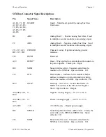
The signals on the rear signal connector can be classified as analog output signals, digital I/O
signals, or timing I/O signals. Signal connection guidelines for each of these groups are given in
the following section.
Analog Output Signal Connections
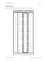
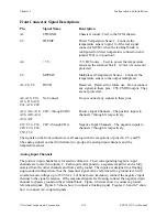
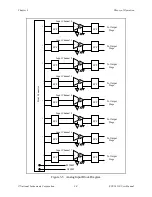
Pins 1 through 19 of the rear signal connector are analog output signal pins. Pins 1 and 2 are
AOGND signal pins. AOGND is an analog output common signal that is routed through jumper
W46 to the analog reference on the SCXI-1120. You can use these pins for a general analog
power ground tie point to the SCXI-1120 if necessary. In particular, when using differential
input data acquisition boards, such as the MIO-16 board, it is preferable to leave jumper W46 in
its factory setting or in position AB-R1 to avoid ground loops. With data acquisition boards that
are configured for referenced single-ended (RSE) measurements, jumper W46 should be in
position AB-R0 to connect the SCXI-1120 analog ground reference to the data acquisition analog
ground. Pin 19 is the OUTREF pin, and is connected internally to the analog reference when
jumper W46 is in position AB-R2. Pins 3 through 18 are the analog output channels of the
SCXI-1120. Pins 3 and 4, or MCH0
±
, are a multiplexed output of all eight channels and the
temperature sensor output. Pins 5 through 18, or MCH1
±
through MCH7
±
, are a parallel
connection of channels 1 through 7 to the rear signal connector. Pin 18 is a direct connection to
the temperature sensor when jumper W41 is in position 3. Notice that the temperature sensor is
located on the terminal block. For further details on configuring the temperature sensor output,
refer to the SCXI-1320 and SCXI-1328 Terminal Blocks section earlier in this chapter.
Warning: The SCXI-1120 analog outputs are not overvoltage protected. Applying external
voltage to these outputs can result in damage to the SCXI-1120. National
Instruments is not liable for any damages resulting from such signal connections.
Note: The SCXI-1120 analog outputs are short-circuit protected.
Digital I/O Signal Connections
Pins 24 through 27, 29, 33, 36, 37, and 43 constitute the digital I/O lines of the rear signal
connector. They are divided into three categories–the digital input signals, the digital output
signals, and the digital timing signals.
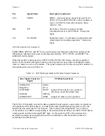
The digital input signals are pins 24, 25, 27, 29, 33, and 37. The data acquisition board uses
these pins to configure the SCXI module that is under data acquisition board control. Each
digital line emulates the SCXIbus communication signals as follows:
•
Pin 25 is SERDATIN and is equivalent to the SCXIbus MOSI serial data input line.
•
Pin 27 is DAQD*/A and is equivalent to the SCXIbus D*/A line. It indicates to the module
whether the incoming serial stream on SERDATIN is data (DAQD*/A = 0) or address
(DAQD*/A = 1) information.
•
Pin 29 is SLOT0SEL* and is equivalent to the SCXIbus INTR* line. It indicates whether the
data on the SERDATIN line is being sent to Slot 0 (SLOT0SEL* = 0) or to a module
(SLOT0SEL* = 1).
•
Pins 24 and 33 are the digital ground references for the data acquisition board digital signals
and are tied to the module digital ground.
• Pin 37 is SERCLK and is equivalent to the SCXIbus SPICLK line and is used to clock the
serial data on the SERDATIN line into the module registers.

